Download presentation
Presentation is loading. Please wait.

1
ECE 498 Frequency Division Multiplexing On PCB (Printed Circuit Board) Science and Engineering Project Center Department of Electrical and Computer Engineering Seattle University
 Science and Engineering Project Center Department of Electrical and Computer Engineering Seattle University")
2
Frequency Division Multiplexing On On PCB (Print Circuit Board) PCB (Print Circuit Board) ECE 498 Team Members: Kun-Chin Chien Michael Mitchell Coord. Advisor: Dr. Al Moser Dr. Al Moser Faculty Advisor: Dr. Robert G. Heeren

3
Our Goal Incorporation of a FDM circuit onto a PCB to allow students to aim their focus on the study of signal flow

4
Overview Project Specifics FDM Laboratory Winter Quarter 05 Replacement multiplier IC New PSpice schematic and PCB layout

5
Project Steps: 1.Design of Low Pass & Band Pass Filters 2.Research a PSpice model for the IC and build the complete schematic into PSpice 3.Research designs for PCB Footprints 4.Create the Netlist to be imported into OrCad Layout Plus 5.Design the PCB layout 6.Route the PCB layout

6
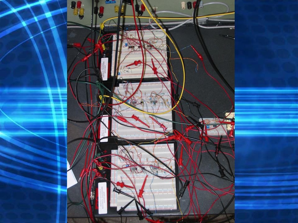
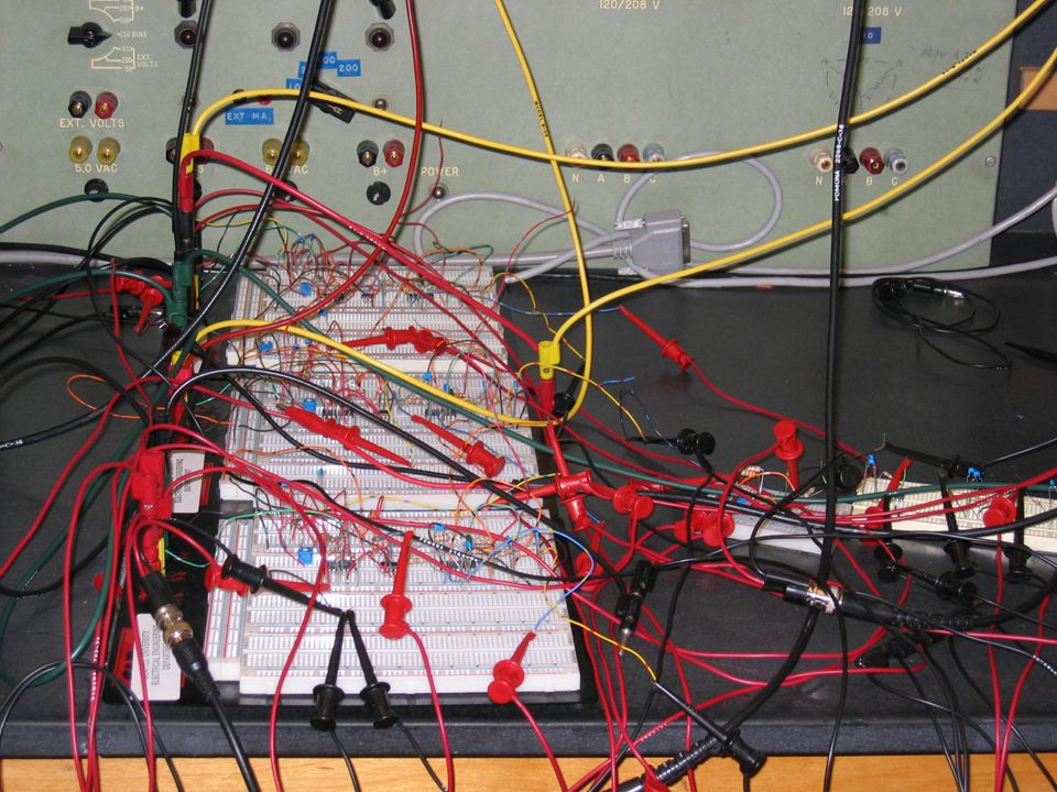
FDM Laboratory Overview FDM Laboratory Overview

9
FDM Schematic With IC MC1496

10
Analog Devices Analog Multiplier AD633JN

11
ModulatorDemodulator Adder Band Pass Filter Low Pass Filter FDM Schematic With IC AD633JN

13
Foot Print of the Banana Plug Jack

14
AMP BNC Connector AMP 222132-1

15
Foot Print of the Bayonet Neill Concelman

16
Foot Print of the Variable Resistor

17
Layout of the Circuit (Using OrCad Layout Plus)
")
18
Layout of the Circuit (Un-routed)
")
19
Layout of the Circuit (6 Layers)
")
20
-15V Input 1 Input 2 Carrier Adder Test Point Output 1 Output 2 +10V -10V +15V Modulator Demodulator BPF LPF 2 Layers

21
Manufactured Price Of the PCB Number of Layers Price 2500 41000 61800 82300 102700 Size of the Board 4.925in(L) X 3.6in(W) Price is dependent on the number of layers, not the number of boards
 X 3.6in(W) Price is dependent on the number of layers, not the number of boards")
22
ECE 498 Conclusion

23
Questions ????

24
Thank you for your attention!

Similar presentations


 Prof. David Parent Group Members:Marcella.>")


>")
 Taylor Nash, Rey Perez, Victor Pinones,>")
 – EE Anna Grimley – EE Mike Kinsella – CPRE Jake Kyro - EE Advisor: Professor Wang.>")


