Download presentation
Presentation is loading. Please wait.

1
CHAMP ASIC: Hawai‘i part
Chicago-Hawai'i ASIC Multi-Purpose Test-structures to evaluate/get experience with IBM 130nm process Building blocks for future runs Hawai'i designers: Matt Andrew (DFF, VCDL/VCRO) Wei Cai (CSA) Mike Cooney (LVDSr) Kurtis Nishimura (WFS) Larry Ruckman (CMP, DAC)
 Wei Cai (CSA) Mike Cooney (LVDSr) Kurtis Nishimura (WFS) Larry Ruckman (CMP, DAC)")
2
CHAMP ASIC: Shared floorplan

3
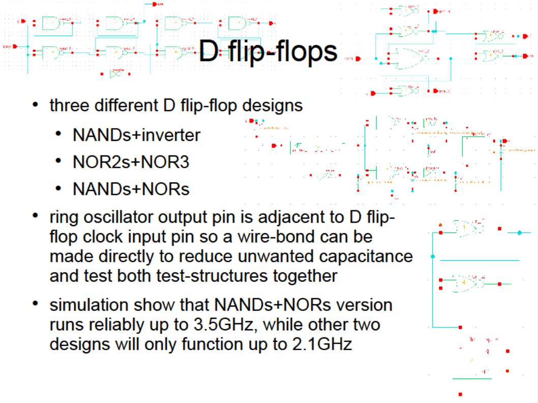
CHAMP ASIC: Hawai‘i design elements
voltage-controlled delay lines, ring oscillator comparator (tested as Wilkinson output from storage array) analog switch (tested as input switch to waveform sampling array - 4 designs) D flip-flop (3 designs) LVDS receiver charge-sensitive amplifier 12-bit transparent latch SPI DAC
 analog switch (tested as input switch to waveform sampling array - 4 designs) D flip-flop (3 designs) LVDS receiver. charge-sensitive amplifier. 12-bit transparent latch SPI DAC.")
4
12-bit DAC R/2R ladder FPGA controlled via SPI
functionality and linearity testable by measuring output voltage with ADC controlled by FPGA

5
comparator (tested with storage array + Wilkinson)
16 storage capacitors column address is set by FPGA row of 4 output channels = 4 Wilkinson outputs timing must be precisely measured to do Wilkinson TDC conversion to verify comparator functionality 1 us long ramp 20 uA CMPbias

6
charge-sensitive amplifier
straightforward to test: put a known quantity of charge in, get voltage signal out digitized by ADC do this with a variety of input signals to determine analog bandwidth

7
analog switch (tested with waveform sampler)
differential input (2 SMAs): coplanar waveguide transmits signal to sampling array 4 channels: 4 sampling capacitor values & switch sizes to investigate optimum parameters to maximize analog bandwidth
: coplanar waveguide transmits signal to sampling array. 4 channels: 4 sampling capacitor values & switch sizes to investigate optimum parameters to maximize analog bandwidth.")
8
analog switch (tested with waveform sampler)
choose sampling rate with 2 analog voltages FPGA must precisely control transfer from sampling cap through differential amplifier to storage cap

9
voltage-controlled delay lines & ring oscillator
two 64-stage VCDLs: one VCDL with regular transistors one with low-threshold voltage (low-Vt) transistors ring oscillator: an 11- stage copy of the low-Vt VCDL, but with feedback so it oscillates
 transistors. ring oscillator: an 11- stage copy of the low-Vt VCDL, but with feedback so it oscillates.")
10
voltage-controlled delay lines & ring oscillator
VCDL testable by measuring delay between input and output signal with an oscilloscope or FPGA for many control voltage value pairs plotting delay vs control voltage difference will provide: lookup table of sampling frequency vs control voltage input+output pad + board trace capacitance ring oscillator testable by setting control voltage pair and measuring output frequency with oscilloscope or FPGA

12
LVDS receiver differential input, single-ended output
testable with FPGA alone: no analog in/out required, except for a bias voltage set with a DAC or potentiometer

13
CHAMP_eval test board ASICs due back ~December
Schematics completed, layout in next couple of weeks Re-use USB2 link hardware/firmware of other test cards

Similar presentations