Download presentation
Presentation is loading. Please wait.

1
Low-power Design at RTL level Mohammad Sharifkhani

2
Motivation All efficient low-power techniques that has been introduced depends on: – Technology enhancement – Specific Standard Cell Library – Analog Design Support This means – Higher cost – Longer design time – Sometimes less reliable product

3
Motivation At RTL we may reduce the number of transition through simple and smart ideas – Mostly affects dynamic power effective capacitance Methods : Too many to count A number of them are standardized in EDA tools (Synopsys DC)
")
4
Motivation

6
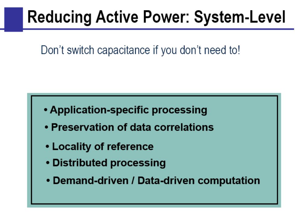
Introduction Signal coding Clock gating Double edge clocking Glitch reduction Operand Isolation Pre-computation concurrency Insertion Parallelism and Pipelining Algorithm level

7
Signal Coding The amount of power consumption is tightly related to the number of transition A combination of bits create a concept for a digital signal (e.g., a number, an address, a command, state of an FSM, …) – Consider it when it runs over a long bus We may take the advantage of the properties of this concept to save the number of transition that we need to communicate it – What does WinZip do?
 – Consider it when it runs over a long bus We may take the advantage of the properties of this concept to save the number of transition that we need to communicate it – What does WinZip do")
8
Signal Coding Some codes are never used

9
Signal Coding

14
Hamming Distance between two consecutive codes: complexity

15
Signal Coding An improvement consists of making the guess that if the most significant bit (MSB) is “1,” the inverted code should be transmitted. The MSB = “1” can be used as the polarity information. Thistechnique is efficient when the vector to transmit is a 2’s complement arithmetic data bus, with MSB being the sign bit.

16
Signal Coding Very often, the value transmitted on a bus (an address bus, for instance) is simply the previous value with an increment. Therefore, the lines can remain the same (i.e., no power consumption) as long as the codes are consecutive, which is mentioned to the receiver by an additional control signal. We may also extend this approach to other known high probably sequences (0000 to 1010 in a given design)
 as long as the codes are consecutive, which is mentioned to the receiver by an additional control signal. We may also extend this approach to other known high probably sequences (0000 to 1010 in a given design).")
17
Signal Coding

19
FSM state encoding scheme – Most of the times the code we use to represent a state is arbitrary let’s choose it in a low-power manner minimal transition between the states We should minimize the hamming distance of the transition with high probability.

20
Signal Coding State encoding: From RESET to S29 are chained sequentially with 100% probability of transition a gray encoding is the best choice. If we assume that condition C0 has a much lower probability than C1, the gray encoding should be not be incremented from S29 to S30 and S31.

21
Signal Coding What we gain in the next-state logic might be lost in the output logic activity trade-off The power reduction on the output logic Common choice: “one hot” encoding to optimize speed, area, and power for the output logic Only valid for a small FSM (i.e., less than 8 to 10 states) because of the large state register A good practice is to group states that generate the same outputs and assign them codes with minimum hamming distance.
 because of the large state register A good practice is to group states that generate the same outputs and assign them codes with minimum hamming distance.")
22
Signal Coding What does it do? (I: input, Y: output) The encoding proposed achieves both a minimum “next-state logic” activity due to the “gray-like” encoding No power consumption at all in the output logic because the orthogonal encoding defines the most significant bit of the state register as the flag Y itself.
 The encoding proposed achieves both a minimum next-state logic activity due to the gray-like encoding No power consumption at all in the output logic because the orthogonal encoding defines the most significant bit of the state register as the flag Y itself..")
23
Introduction Signal coding Clock gating Double edge clocking Glitch reduction Operand Isolation Pre-computation concurrency Insertion Parallelism and Pipelining Algorithm level

24
Clock gating Clock signal: – Highest transition probability – Long lines and interconnections – Consumes a significant fraction of power (sometimes more than 40% if not guarded) Idea: gate the clock if is not needed Popular and standardized in EDA tools
 Idea: gate the clock if is not needed Popular and standardized in EDA tools")
30
Clock gating We can gate the clock of FFs if the output value of A is not needed Saves the power in: – Clock tree – Fan-out of FF (A) – FF themselves Can be implemented in: – Module level – Register level – Cell level A(x) CLK X
 – FF themselves Can be implemented in: – Module level – Register level – Cell level A(x) CLK X")
31
Clock gating

32
To eliminate the glitches on CLKG a latched based approach is favorable – An alternative and better solution : a latch L transparent (when the clock is low) and an AND gate. With this configuration, the spurious transitions generated by function Fcg (clock gating function) are filtered.
 are filtered..")
33
Clock gating

34
Example: The clock-gating file and the register file : physically close to reduce the impact on the skew and to prevent unwanted optimizations during the synthesis. They can be modeled by two separate Processes (VHDL) in the same hierarchical block, synthesized, Then inserted into the parent hierarchy with a “don’t touch” attribute.
 in the same hierarchical block, synthesized, Then inserted into the parent hierarchy with a don’t touch attribute..")
35
Clock gating Reduced area and power Testability and clock skew

36
Clock gating Timing issues: setup time or hold time violations. In most power design flows, the clock gating is inserted before the clock tree synthesis. – the designer has to estimate the delay impact of the clock tree from the clock gate to the gated register as depicted. – by setting some variables allow the designer to specify these critical times before synthesis.

37
Clock gating The skew between A and B creates a Glitch Clock skew must be less than Clock to output delay of the latch Clock skew must be less than Clock to output delay of the latch Positive skew on B (B later than A) can create glitch if not controlled!
 can create glitch if not controlled!")
38
Clock gating The skew between A and B creates a Glitch Negative skew on B (B earlier than A) can create glitch if not controlled! If B comes earlier than the correct EN1 appears at AND input, it creates a glitch

39
Clock gating Testability issues – Clock gating introduces multiple clock domains in the design no clock during the test phase – One way to improve the testability of the design is to insert a control point, which is an OR gate controlled by an additional signal scan_mode. – Its task is to eliminate the function of the clock gate during the test phase and thus restores the controllability of the clock signal.

40
Clock gating How to find a group of FF for gating: Hold condition detection: Flip-flops that share the same hold condition are detected and grouped to share the clock-gating circuitry. This method is not applicable to enabled flip-flops. Redundant-clocking detection: The method is simulation-based. Flip-flops are grouped with regard to the simulation traces to share the clock- gating circuitry. It is obvious that this method cannot be automated.

41
Clock gating In FSM clock gating can be used efficiently: – It is not useful to have switching activity in the next-state logic or to distribute the clock if the state register will sample the same vector

42
Clock gating Example: A FSM that interacts with a timer-counter to implement a very long delay of thousands of clock cycles before executing a complex but very short operation (in the DO_IT state). We can use the clock-gating techniques to freeze the clock and the input signals as long as the ZERO flag from the time-out counter is not raised. Efficient because: – FSM spends most of the time in the WAIT state. – More efficient if the FSM is used to control a very large datapath which outputs will not be used in the WAIT state. We can gate the clock or mask the inputs of this datapath and, therefore, avoid dynamic power consumption during all the countdown phases. It is the RTL designer’s task to try to extract these small subparts of the FSM, isolate them, and then freeze the rest of the logic that is large and that most of the time does not achieve any useful computation.

43
Clock gating FSM partitioning can be applied to adopt clock gating: – Subroutines in software part of an FSM may only be called in certain conditions we can separate it and gate its clock Other words: Decompose a large FSM into several simpler FSMs with smaller state registers and combinatorial logic blocks. Only the active FSM receives clock and switching inputs. The others are static and do not consume any dynamic power.

44
Clock gating We can easily partition the big FSM into two parts and isolate the subroutine loop. We add a wait state, SW22 and TW0, between the entry and exit points of the subroutine in both FSMs. Mutually exclusive FSMs (when one is running the other is off)
.")
45
Clock gating

46
Introduction Signal coding Clock gating Double edge clocking Glitch reduction Operand Isolation Pre-computation concurrency Insertion Parallelism and Pipelining Algorithm level

47
Double edge clocking Major constraint for a digital system is throughput (bps: read it op/sec) For a given architecture: – The number of ‘clock cycles in a second’ is a linear function of throughput: One operation/clock cycle – For a given throughput (op/sec) the amount of energy/sec is fixed Every ‘clock cycle’ consumes constant power on clock tree (cycle includes positive and negative) Idea: we can half the clock tree power if we double the number of operation in a given ‘clock cycle’ double edge clocking
 For a given architecture: – The number of ‘clock cycles in a second’ is a linear function of throughput: One operation/clock cycle – For a given throughput (op/sec) the amount of energy/sec is fixed Every ‘clock cycle’ consumes constant power on clock tree (cycle includes positive and negative) Idea: we can half the clock tree power if we double the number of operation in a given ‘clock cycle’ double edge clocking")
48
Double edge clocking Double edge triggered FF – Static – Dynamic Zero threshold voltage for MOS is assumed

49
Double edge clocking The ratio of the SET to DET FF energy consumption is: – (2n+3)/(2n+2). Circuit simulation for a random vector:

50
Double edge clocking The energy consumption for SET and DET registers are Higher pipelining order, better Higher clock rate, better

51
Double edge clocking Ripple carry adder followed by a set of registers – For a given throughput the DET offers less power consumption

52
Double edge clocking What is this? How it saves power compared to the regular implementation?

53
Introduction Signal coding Clock gating Double edge clocking Glitch reduction Operand Isolation Pre-computation concurrency Insertion Parallelism and Pipelining Algorithm level

54
Glitch reduction Glitch: The output of a combinational logic settles to the right value after a number of transitions between 1 and 0 Example: Parity of the output of a ripple carry adder when it adds ‘111111’ with ‘000001’. Because of the parasitic capacitive coupling, glitches also affect the signal integrity and the timing closure Glitch propagates!

55
Glitch reduction Idea1: Use FF before you let a glitch propagate – Latency, control logic, more FF, clock tree, etc. Latency may be a show stopper when specific requirements are demanded Idea2: Use multi-phase clocking system: – Two phase master slave latch – Extra clock generation and routing overhead

56
Glitch reduction Idea3: balance the delay in parallel combinatorial paths – Problematic when there is device variation in scaled CMOS Idea4: use sum of product instead of generating the output based on casecade of multiple blocks : set_flatten true in the synthesis – Power and area – Example: for the parity in the above example, we may extract the parity directly from the input instead of an adder and XOR tree

57
Glitch reduction Make use of naturally glitch resilient logic styles: – Domino style for example – Requires a dedicated library of cells and an additional clock signal. To map the RTL code, we can again use direct instances or synthesis scripts to control the inferences (e.g., set_dont_use and set_use_only).
..")
58
Glitch reduction Block reordering – Area is compromised, sometimes even power – Investigation is needed mux Glitch mux

59
Introduction Signal coding Clock gating Double edge clocking Glitch reduction Operand Isolation Pre-computation concurrency Insertion Parallelism and Pipelining Algorithm level

60
Operand Isolation Block the operands to get through the (arithmetic) datapath if not needed
 datapath if not needed")
61
Operand Isolation

62
Example our multi-standard crypto-processor:

63
Operand Isolation Control signal gating – Helps to reduce the switching on the buses A Power Management Unit (PMU) is employed to decide which bus is truly needed to take a value – The rest of the busses remain inactive
 is employed to decide which bus is truly needed to take a value – The rest of the busses remain inactive")
64
Operand Isolation When enb is not active, mux_sel, reg1_en, and reg2_en can be gated, leading to a 100% switching activity reduction in R_Bus, A_bus, and B_Bus. When mux-sel is active, either reg1_en and reg2_en can be gated depending on the value of mux-sel.

65
Introduction Signal coding Clock gating Double edge clocking Glitch reduction Operand Isolation Pre-computation concurrency Insertion Parallelism and Pipelining Algorithm level

66
Precomputation

67
g1 and g2 are predictor functions which are – Mutually exclusive – Simpler than f Affects the speed a bit (applied to non critical path) Maximum probability of g1 or g2 becomes active is desired – Choice of g1, g2
 Maximum probability of g1 or g2 becomes active is desired – Choice of g1, g2")
68
Precomputation Partitioning the inputs to block A – Some of the inputs can be masked The rest will do f A power reduction is achieved because only a subset of the inputs to block A change implying reduced switching activity. Less delay is imposed

69
Precomputation Clearly, when g1 = 1, C is greater than D, and when g2 =1,C is less than D. We have to implement

70
Introduction Signal coding Clock gating Double edge clocking Glitch reduction Operand Isolation Pre-computation concurrency Insertion Parallelism and Pipelining Algorithm level

71
Sometimes a job can be done in different way – Different algorithms – Different architectures Design with power in mind – Lease switching activity in mind Sometimes priory knowledge about the nature of the signals would be of help – DSP applications

72
Algorithm level Adds only positive values Adds only negative values Signal activity at different bits

73
Algorithm level

74
Introduction Signal coding Clock gating Double edge clocking Glitch reduction Operand Isolation Pre-computation concurrency Insertion Parallelism and Pipelining Algorithm level

75
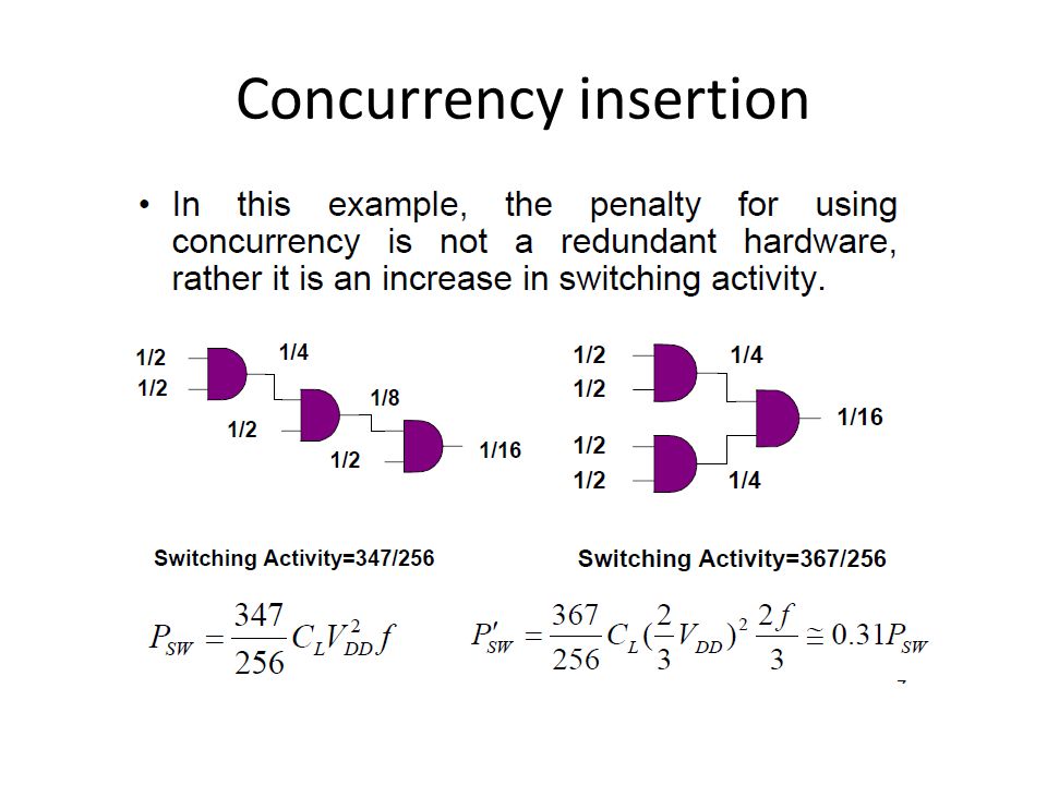
concurrency Insertion High enough speed (throughput) can be traded off with power – Lower supply voltage – Particularly useful in off critical path (where the speed is not important) All hierarchical high throughput architectures can be treated as a low-power approach! – Concurrency insertion – Parallelism – Pipelining

76
concurrency insertion

77
Concurrency insertion

79
Introduction Signal coding Clock gating Double edge clocking Glitch reduction Operand Isolation Pre-computation concurrency Insertion Parallelism and Pipelining Algorithm level

80
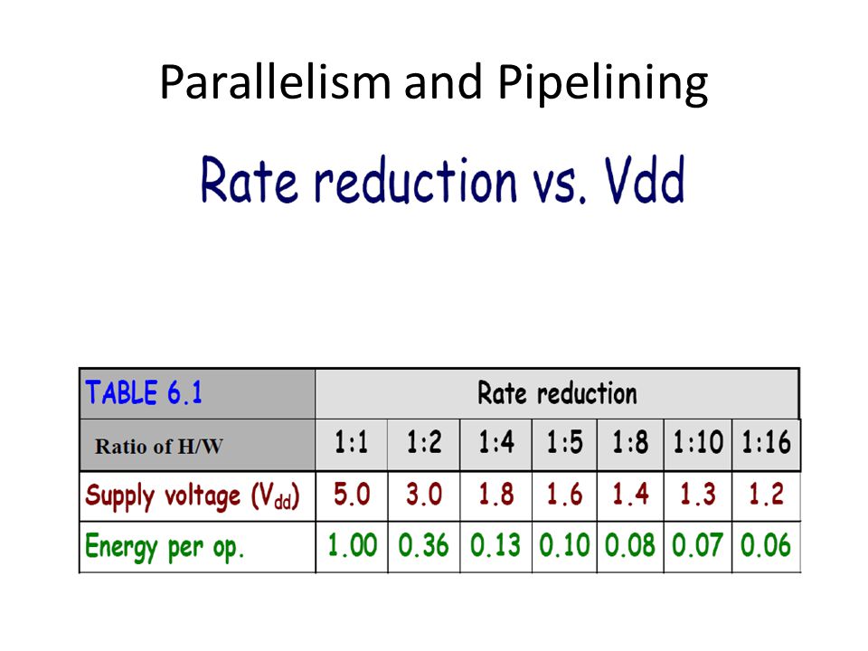
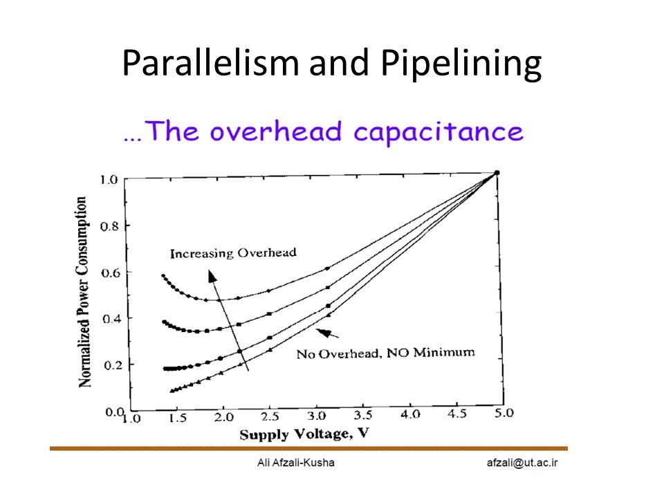
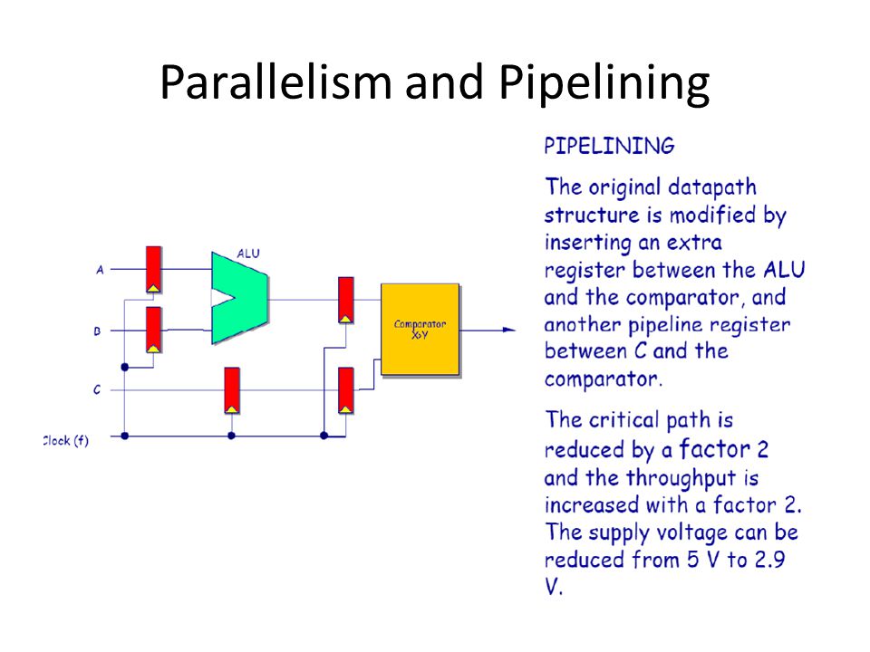
Parallelism and Pipelining Exploit parallel processing to achieve higher throughput and trade it off with lower supply voltage

81
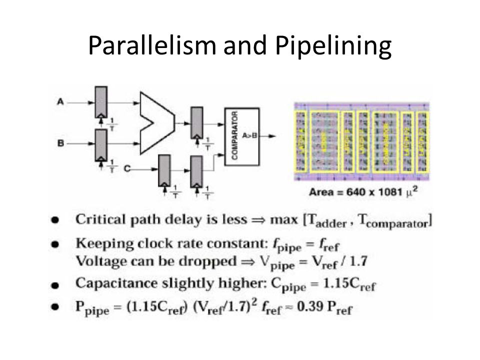
Parallelism and Pipelining

89
A longer cycle time is needed for each processor because of the lower voltage. A longer cycle time is needed for each processor because of the lower voltage.

90
Parallelism and Pipelining

99
Conclusion

Similar presentations


 n Test.>")


>")
 Computer Architecture Computer Architecture.>")


