Download presentation
Presentation is loading. Please wait.

1
E-beam litografi Nano imprint litografi
Nanolitografi E-beam litografi Nano imprint litografi

2
Mikroskopi

3
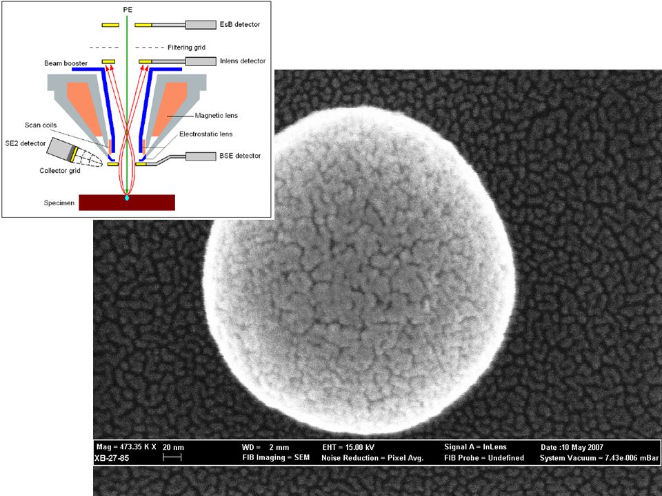
SEM (scanning electron microscope)
")
4
Komponenter i SEM Schottky emitter elektronkilde Magnetisk linse
F =-e v x B Magnetisk linse

9
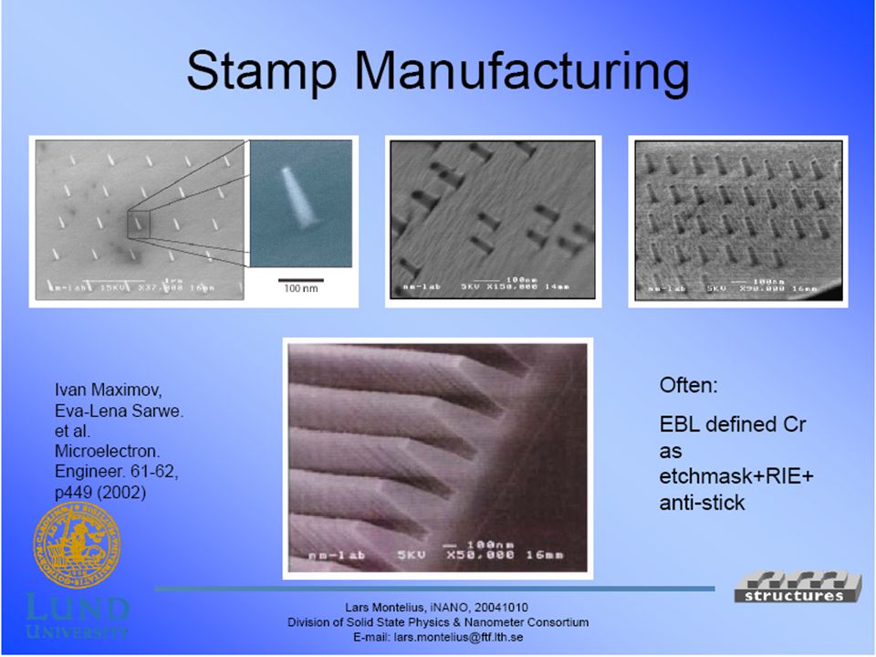
E-beam litografi - Dedikerede e-beam systemer
- SEM med Raith Gmbh kontrolsystem og ’pattern generator’ DANCHIP

10
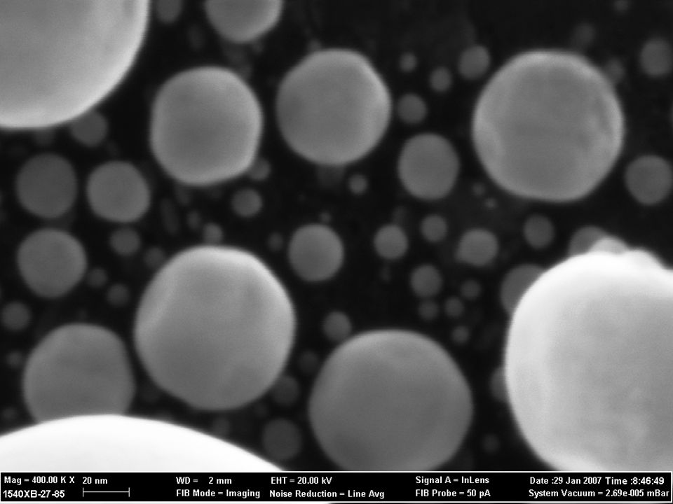
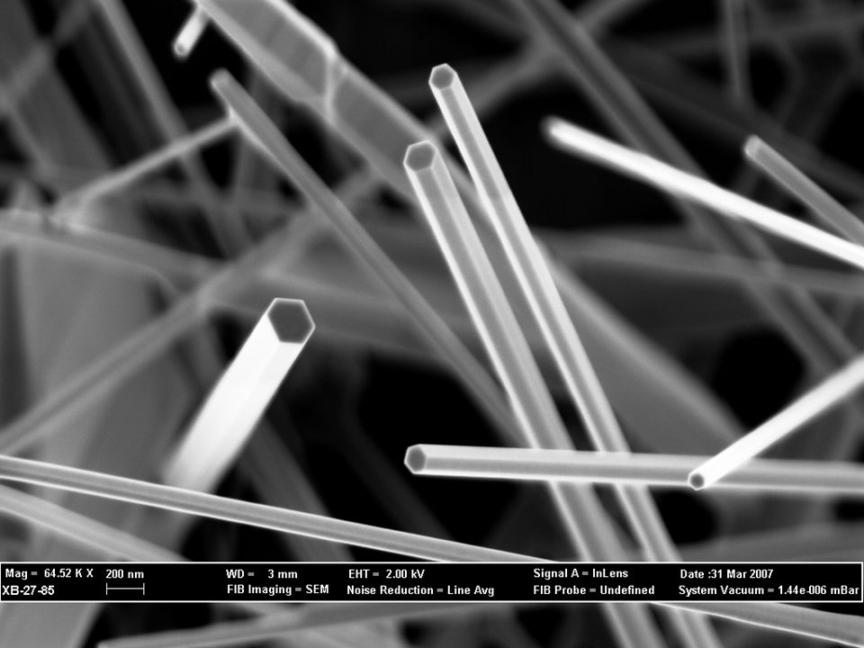
Test of nanowire writing E-beam writing+RIE (Nano 9 – Tom+Jeppe)
")
11
Wires and channels

12
Diffraktive komponenter
Optiske strukturer Diffraktive komponenter 2D grating: Periodicity - 250nm

13
Nano Imprint Lithography (NIL)
")
17
Nanowire detektor Appl. Phys. Lett. 89, (2006)
")
18
Focused Ion Beam (FIB) System
 System")
19
Focused Ion Beam Writing
As the diagram on the right shows, the gallium (Ga+) primary ion beam hits the sample surface and sputters a small amount of material, which leaves the surface as either secondary ions (i+ or i-) or neutral atoms (n0). The primary beam also produces secondary electrons (e-). As the primary beam rasters on the sample surface, the signal from the sputtered ions or secondary electrons is collected to form an image.
 primary ion beam hits. the sample surface and sputters a small. amount of material, which leaves the. surface as either secondary ions (i+ or i-) or neutral atoms (n0). The primary beam. also produces secondary electrons (e-). As the primary beam rasters on the sample. surface, the signal from the sputtered ions. or secondary electrons is collected to form. an image.")
20
E-beam og FIB litografi
E-beam ~10 nm FIB ~20 nm EDX

21
TEM samples

22
FIB skrivning AAU-logo på et hår

23
CVD med FIB stråle Shinji MATSUI

29
FIB skrivning AAU-logo på et hår

Similar presentations


 for magneto-optics Paolo Vavassori INFM - National Research Center on nanoStructures and Biosystems at Surfaces.>")


 1.Overview. 2.Ion source and optics. 3.Ion-solid interaction, damage. 4.Scanning ion beam imaging. ECE 730: Fabrication in the nanoscale:>")


 Overview. Ion source and optics.>")

>")


 Sam de Poortere, Ariel Riveros, Lauren Kelly, Mariella Piacenti, Irina Erickson & Tom Hughes.>")


 Applying Atomic Structure Knowledge to Chemical Analysis.>")