Download presentation
Presentation is loading. Please wait.

1
Bandgap Engineering of the Amorphous Wide Band-Gap Semiconductor (SiC)1-x(AlN)x Doped with Rare Earths and its Optical Emission Properties Roland Weingärtner San Miguel, 14th of April 2011 Departamento de Ciencias – Sección Física – Grupo Ciencias de los Materiales Pontificia Universidad Católica del Perú (PUCP)
")
2
Outline I Motivation and Introduction Wide band-gap semiconductors
Band-gap engineering Rare earth doping and optical emission II First Results of a-(SiC)x(AlN)1-x Thin film growth method and structural characterisation Band-gap engineering of a-(SiC)x(AlN)1-x III Cathodoluminescense measurements Spectral emission of rare earth doped a-(SiC)x(AlN)1-x Thermal activation of rare earth emission IV Summary and Acknowledgements
x(AlN)1-x. Thin film growth method and structural characterisation. Band-gap engineering of a-(SiC)x(AlN)1-x. III Cathodoluminescense measurements. Spectral emission of rare earth doped a-(SiC)x(AlN)1-x. Thermal activation of rare earth emission. IV Summary and Acknowledgements.")
3
Why wide band-gap semiconductors ?
Principal idea: Combine the advantages of an insulator and a semiconductor Advantage of a semiconductor: Active electronic devices like diodes, transistors, etc Advantage of an insulator: Due to the wide band-gap the samples are transparent Historic development: GaN based LED

4
Example: Silicon Carbide (c-SiC)
High power electronics: Schottky diode with high breakdown voltage Reduction of space and costs in a power source unit of a PC Band gap Breakdown voltage SiC 3.0 eV 5 MVcm-1 Si 1.1 eV 0.3 MVcm-1 Other applications: optoelectronics High frequency electronics High temperature devices

5
Band-gap engineering AxB1-x The band-gap has influence on:
Emission wavelength of an optical device efficiency of the light emission energy level of the dopants etc. AxB1-x Variation of the band-gap by changing the composition Choose an optimal composition for a specific application

6
Small overview of semiconductors
Wide band-gap

7
Why rare earth doping in semiconductors ?
Optical emission properties of rare earths: emission wavelength does not depend on the host material Color is typical for a specific rare earth ion Intensity of rare earth emission depends on the material: band-gap quenching temperature quenching concentration quenching

8
Colors in rare earth doped GaN
M. Garter et al. Appl. Phys. Lett. 74 (1999) p.182
 p.182.")
9
Cathodoluminescense of RE3+
Excitation mechanism Cathodoluminescense of RE3+ in a-AlN:RE Intrashell-transitions of f-shells RE3+ Ion 1 and 2: excitation paths a and b: recombination paths

10
Temperature quenching of Er3+ doped semiconductors
In0,16Ga0,38As0,84P0,16 Si InP GaAs Al0,17Ga0,83As ZnTe CdS Increase of band-gap From Favennec: Electronics Letters 25 (1989) 718
 718.")
11
Temperature quenching for Er3+ emission
From Zanatta: Appl. Phys. Lett (2003)
")
12
Temperature quenching in AlN:RE
Phenomenological description: From Lozykowski and Jadwisienczak: Phys. Stat. Sol. B 244 (2007) 2109
")
13
Outline I Motivation and Introduction Wide band-gap semiconductors
Band-gap engineering Rare earth doping and optical emission II First Results of a-(SiC)x(AlN)1-x Thin film growth method and structural characterisation Band-gap engineering of a-(SiC)x(AlN)1-x III Cathodoluminescense measurements Spectral emission of rare earth doped a-(SiC)x(AlN)1-x Thermal activation of rare earth emission IV Summary and Acknowledgements
x(AlN)1-x. Thin film growth method and structural characterisation. Band-gap engineering of a-(SiC)x(AlN)1-x. III Cathodoluminescense measurements. Spectral emission of rare earth doped a-(SiC)x(AlN)1-x. Thermal activation of rare earth emission. IV Summary and Acknowledgements.")
14
a-(SiC)x(AlN)1-x:RE Why a-(SiC)x(AlN)1-x? Wide bandgap semiconductors:
Increase of rare earth emission Lower temperature quenching Transparent Semiconductor devices Rare earth doping: Well defined emission color Covering of the whole color range a-(SiC)x(AlN)1-x:RE Amorphous films: Inexpensive Simple production Higher incorporation of rare earths Pseudobinary compound: Band-gap engineering (3eV to 6eV) one composition parameter Sputtering from SiC and AlN target
x(AlN)1-x:RE. Amorphous films: Inexpensive. Simple production. Higher incorporation of rare earths. Pseudobinary compound: Band-gap engineering (3eV to 6eV) one composition parameter. Sputtering from SiC and AlN target.")
15
Los principios de dc-sputtering
target sustrato + 10-2 mbar + + 1000 V + + + + ánodo + + ion Ar Átomo Ar electrón Plasma frío: Problemas: Inestabilidad del plasma Sólo targets metálicos Baja eficiencia

16
Los principios de magnetrón-sputtering
Aumento de densidad de los iones Más rapidez del crecimiento

17
El magnetrón portatarget blindaje Anillo de plasma target
magnetrón armado S N S S N N

18
Schematics of the sputtering system
Mass spectrometer Control of mass spectrometer H2O shutter Mass flow controler substrate targets Pressure sensor Rf- generator Rf-generator flexible magnetrons Turbo-molecular pump H2O match Mechanical pump control PC control Ar N2

19
The rf magnetron sputter system at the PUCP
Vacuum system: residual gas analysis Gas processing: flow control of N2, H2 and Ar: …100 sccm, 5N...6N working pressure: Sputter targets: trial magnetron sputtering, 2´´ 3 Rf generators, P<300W felxible target geometry !! Substrates: Substrate area up to 128 cm2 variable target substrate distance water cooled substrate holder

20
A typical film of a-SiC on glas
Target material: Silicon Carbide (SiC) Substrate material: fused glas Rf power: 100 W Process gas: Argon, 5N Gas flow: 80 sccm Argon pressure: 810-3 mbar 3´ a-SiC 3´
 Substrate material: fused glas. Rf power: 100 W. Process gas: Argon, 5N. Gas flow: 80 sccm. Argon pressure: 810-3 mbar. 3´ a-SiC. 3´")
21
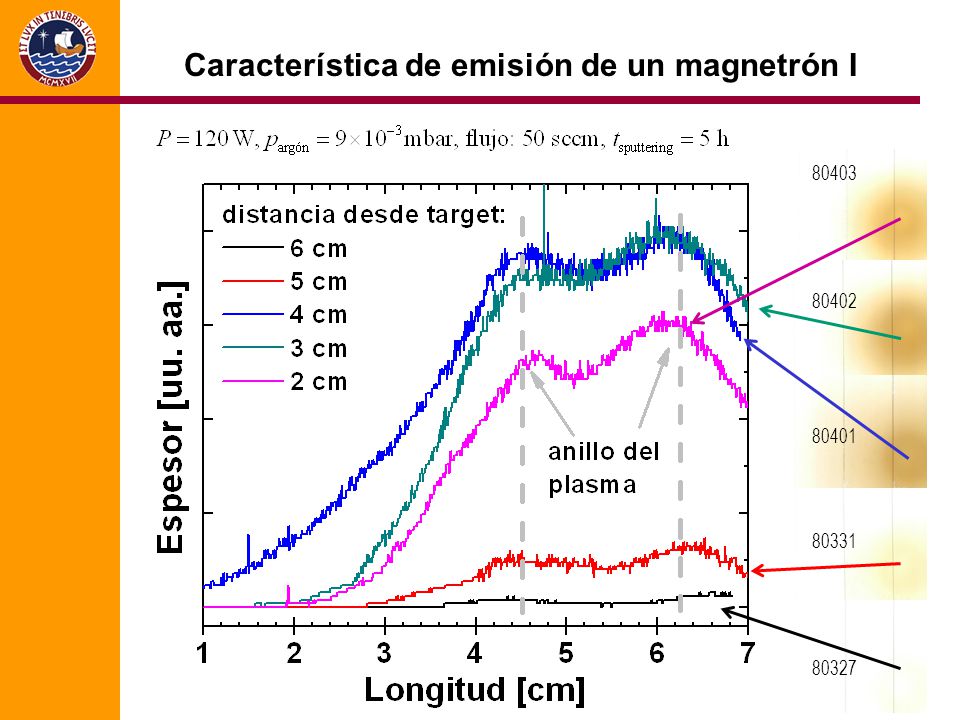
Característica de emisión de un magnetrón I
80403 80402 80401 80331 80327
22
Característica de emisión de un magnetrón II
emisión en uu. aa. Contorno de emisión 1cm plasma target S N S blindaje S N N imanes

23
A typical thin film of a-(SiC)x(AlN)1-x
EDX results host substrate highly pure films (i.e. Na content < 8 ppm wt.) no signature of impurities in the film
 no signature of impurities in the film.")
24
Structure of a/nc-AlN and a-SiC anealed at 900°C
Transmission electron microscopy (TEM): diffraction a/nc-AlN a-SiC Substrate (Si) High resolution transmission electron microscopy (HRTEM): a/nc-AlN There are nanocrystals embedded in an amorphous matrix
: diffraction. a/nc-AlN. a-SiC. Substrate (Si) High resolution transmission electron microscopy (HRTEM): a/nc-AlN. There are nanocrystals embedded. in an amorphous matrix.")
25
Optical absorption measurements
Determination of the band-gap i.e. a-(SiC)0.25(AlN)0.75 :
0.25(AlN)0.75 :")
26
Band-gap engineering of a-(SiC)x(AlN)1-x
[1] Nurmagomedov et al.: Sov. Phys. Semicond (1989) [2] Gurumurugan et al.: Appl. Phys. Lett (1999) [3] Zanatta et al.: J. Phys. D: Appl. Phys. 42 (2009) Fitting to Vegard´s law: Bowing parameters: ba2=(1.98±0.94) eV , bTauc=(1.96±0.48) eV
 [2] Gurumurugan et al.: Appl. Phys. Lett (1999) [3] Zanatta et al.: J. Phys. D: Appl. Phys. 42 (2009) Fitting to Vegard´s law: Bowing parameters: ba2=(1.98±0.94) eV , bTauc=(1.96±0.48) eV.")
27
Outline I Motivation and Introduction Wide band-gap semiconductors
Band-gap engineering Rare earth doping and optical emission II First Results of a-(SiC)x(AlN)1-x Thin film growth method and structural characterisation Band-gap engineering of a-(SiC)x(AlN)1-x III Cathodoluminescense measurements Spectral emission of rare earth doped a-(SiC)x(AlN)1-x Thermal activation of rare earth emission IV Summary and Acknoledgements
x(AlN)1-x. Thin film growth method and structural characterisation. Band-gap engineering of a-(SiC)x(AlN)1-x. III Cathodoluminescense measurements. Spectral emission of rare earth doped a-(SiC)x(AlN)1-x. Thermal activation of rare earth emission. IV Summary and Acknoledgements.")
28
Emission of rare earth ions in a/nc-AlN and a-SiC
Cathodoluminescense of RE3+ in a-AlN:RE Cathodoluminescense of RE3+ in a-SiC:RE

29
Thermal activation of a-/nc-AlN
exponential growth with the anealing temperature there is a saturation of the RE emission at anealing tempertures of 900°C

30
Thermal activation of a-SiC
exponential growth with anealing temperature there is no saturation up to 1000°C there is an optimal anealing temperature for the Tb3+ emission in a-SiC

31
Thermal activation of a-(SiC)x(AlN)1-x
x(AlN)1-x")
32
Thermal activation of a-(SiC)0.83(AlN)0.17:Tb3+
0.83(AlN)0.17:Tb3+")
33
Summary Wide-bandgap semiconductors Rare earth doping
bandgap engineering First results on a-(SiC)x(AlN)1-x thin films HRTEM investigations bandgap engineering of a-(SiC)x(AlN)1-x Cathodoluminescense optical emission of a-(SiC)x(AlN)1-x thermal activation of rare earth emission Conferences/Publications: IMRC 2009 in Cancun, Mexico (invited talk) ICSCRM´2009 in Nuremberg, Germany Five publications in International Journals
x(AlN)1-x thin films. HRTEM investigations. bandgap engineering of a-(SiC)x(AlN)1-x. Cathodoluminescense. optical emission of a-(SiC)x(AlN)1-x. thermal activation of rare earth emission. Conferences/Publications: IMRC 2009 in Cancun, Mexico (invited talk) ICSCRM´2009 in Nuremberg, Germany. Five publications in International Journals.")
34
Acknowledgements Materials Department, University of Erlangen, Germany
Prof. Dr. Winnacker Prof. Dr. H. P. Strunk Catholic University of Lima, Peru (PUCP) Prof. F. De Zela Andrés Guerra, Gonzalo Galvez, Oliver Erlenbach (PhD) Liz Montañez, Katia Zegarra, (Licenciatura) This research work is supported by the Pontificia Universidad Católica del Peru (PUCP) Deutsche Forschungsgemeinschaft (DFG) and the German Service of Academic Interchange (DAAD)
 Prof. F. De Zela. Andrés Guerra, Gonzalo Galvez, Oliver Erlenbach (PhD) Liz Montañez, Katia Zegarra, (Licenciatura) This research work is supported by the. Pontificia Universidad Católica del Peru (PUCP) Deutsche Forschungsgemeinschaft (DFG) and the. German Service of Academic Interchange (DAAD)")
35
Wide bandgap semiconductors
From Steckl MRS Bull. 24, p. 33 (1999)
")
Similar presentations


>")


>")


 Low dimensional materials: Quantum wells,>")

