Download presentation
Presentation is loading. Please wait.

1
MMIC Design in 0.13µm SiGe BiCMOS Process by Hans Schou and Magnus Pallesen

2
IHP SG13S 0.13 µm SiGe HBT BiCMOS 1.2 V HBT with fT=250 GHz 3.3 V HBT with fT=50 GHz 1.2 V logic CMOS 3.3 V I/O CMOS

3
NPN Layout Configurations

4
SG13S Stackup

6
Design of a 60 GHz Low Noise Amplifier in a 0.13 µm SiGe BiCMOS Process By Magnus Pallesen

7
LNA Specifications

8
Design Methodology Determine number of stages, topology and bias. Design as single stages with ideal components. Cascade single stages to multistage amplifier. Replace inductors with T-lines.

9
Topology Preferably both Common Emitter and Cascode Matching problems with Cascode due to high output impedance. CE best alternative.

10
Bias Trade-off between power consumption, gain and noise

11
Multistage design VBB=850 mV Optimized for Low noise VBB=850 mV Medium gain Medium nosie VBB=880 mV Optimized for high gain CE Trade-off between power consumption, noise, bandwidth and gain

12
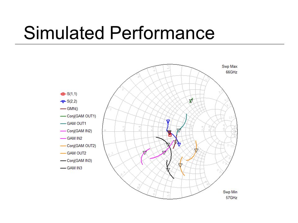
Simulated Performance

14
Post Layout Schematic

15
Layout 320µm 411µm

16
Simulated Performance

18
Design of a 60 GHz Power Amplifier in 0.13 µm SiGe BiCMOS By Hans Schou

19
Power Amplifier Design Goals

20
Class AB operation at VBB=0.85

21
Output Stage Port Parameters High reverse transmission, S12

22
Three Stage Amplifier Three common emitters Tuned for maximum output power

23
Simulated Performance

24
Schematic

26
Simulated Performance

27
Questions?

Similar presentations