Download presentation
Presentation is loading. Please wait.

10
Solution to Obsolete Semiconductors Innovate, Re-create, Manufacture, Test Force Technologies Ltd. Ashley Crt, Henley, Marlborough, Wiltshire SN8 3RH United Kingdom Tel: +44 (0)1264-713200 Fax: +44 (0)1264-731444 www.forcetechnologies.co.uk Frequently Asked Questions – FAQ The first time that someone hears that semiconductor die can be "removed" from any package and "reassembled" into any other package, this typically raises eyebrows. However, our Advanced Extraction Solutions Group routinely uses this approach to solve customers' requirements with consistently excellent results. On a customer by customer basis, we have clearly demonstrated the viability of this approach through empirical data through multiple rounds of successful qualification test results. Here are some of the most Frequently Asked Questions from prospective customers: Question #1: Is this an effective solution for Diminishing Manufacturing Sources and Material Shortages (DMSMS) for military ICs? Response #1: Absolutely! This is frequently an excellent solution for managing Diminishing Manufacturing Sources and Material Shortages (DMSMS) especially when an IC is required that is obsolete or is no longer available in the desired package but where that IC is readily available in other package formats. These other package formats serve as a ready supply of die that can be quickly and easily removed and reassembled into any package format that is desired for the end application. Our ICs have passed all qualification testing to which they have been subjected and they have performed as well or better than the original IC packaged from which the die originated. Question #2: Very few companies offer this service, so failure statistics if available, may have low sample sizes. What are your quality levels? Response #2: It is clearly true that very few companies offer this service. In fact, this is the only company to our knowledge that removes and reassembles IC into different packages. However, we will gladly produce for a customer as many or as few units as they would like to purchase use to populate their own qualification samples. Many ICs for military applications have been qualified to the full battery of MIL-STD-883 testing with 200 or less IC units. We often suggest that a prospective customer first try an evaluation with only 20 units which we would gladly provide at that a reasonable unit price. We respect our customer's preferred approach. Force is quite flexible and we wish to earn our customer's trust that our process is highly reliable and is also the lowest cost solution available compared to alternate solutions (e.g., redesign of an IC or of a PCB/system). The excellent data that is generated from these evaluations will make our case. Question #3: Most prospective IC customers have no historical evidence of die removal other than for failure analysis. Does this work? Response #3: We certainly understand this concern. We also initially started this process for the purpose of failure analysis and found from this that these die were extremely useful and well suited to solve a variety of issues and needs in the industry. This works extremely well. Question #4: Isn't this a unique process for each IC since each die extracted is somewhat different? Therefore, would evidence of failure rates of previously processed parts may be consistent across a larger sample of products? Response #4: We use tightly controlled production processes that are quite repeatable and we see tremendous consistency from unit to unit across multiple lots of material processed and multiple die of various sizes and technologies. Solution to Obsolete Semiconductors Innovate, Re-create, Manufacture, Test Force Technologies Ltd. Ashley Crt, Henley, Marlborough, Wiltshire SN8 3RH United Kingdom Tel: +44 (0)1264-731200 Fax: +44 (0)1264-731444 www.forcetechnologies.co.uk
 Fax: +44 (0) Frequently Asked Questions – FAQ The first time that someone hears that semiconductor die can be removed from any package and reassembled into any other package, this typically raises eyebrows. However, our Advanced Extraction Solutions Group routinely uses this approach to solve customers requirements with consistently excellent results. On a customer by customer basis, we have clearly demonstrated the viability of this approach through empirical data through multiple rounds of successful qualification test results. Here are some of the most Frequently Asked Questions from prospective customers: Question #1: Is this an effective solution for Diminishing Manufacturing Sources and Material Shortages (DMSMS) for military ICs. Response #1: Absolutely. This is frequently an excellent solution for managing Diminishing Manufacturing Sources and Material Shortages (DMSMS) especially when an IC is required that is obsolete or is no longer available in the desired package but where that IC is readily available in other package formats. These other package formats serve as a ready supply of die that can be quickly and easily removed and reassembled into any package format that is desired for the end application. Our ICs have passed all qualification testing to which they have been subjected and they have performed as well or better than the original IC packaged from which the die originated. Question #2: Very few companies offer this service, so failure statistics if available, may have low sample sizes. What are your quality levels. Response #2: It is clearly true that very few companies offer this service. In fact, this is the only company to our knowledge that removes and reassembles IC into different packages. However, we will gladly produce for a customer as many or as few units as they would like to purchase use to populate their own qualification samples. Many ICs for military applications have been qualified to the full battery of MIL-STD-883 testing with 200 or less IC units. We often suggest that a prospective customer first try an evaluation with only 20 units which we would gladly provide at that a reasonable unit price. We respect our customer s preferred approach. Force is quite flexible and we wish to earn our customer s trust that our process is highly reliable and is also the lowest cost solution available compared to alternate solutions (e.g., redesign of an IC or of a PCB/system). The excellent data that is generated from these evaluations will make our case. Question #3: Most prospective IC customers have no historical evidence of die removal other than for failure analysis. Does this work. Response #3: We certainly understand this concern. We also initially started this process for the purpose of failure analysis and found from this that these die were extremely useful and well suited to solve a variety of issues and needs in the industry. This works extremely well. Question #4: Isn t this a unique process for each IC since each die extracted is somewhat different. Therefore, would evidence of failure rates of previously processed parts may be consistent across a larger sample of products. Response #4: We use tightly controlled production processes that are quite repeatable and we see tremendous consistency from unit to unit across multiple lots of material processed and multiple die of various sizes and technologies. Solution to Obsolete Semiconductors Innovate, Re-create, Manufacture, Test Force Technologies Ltd. Ashley Crt, Henley, Marlborough, Wiltshire SN8 3RH United Kingdom Tel: +44 (0) Fax: +44 (0)")
11
Frequently Asked Questions – FAQ Question #5: What failure rates do you see on "removed and reassembled" die? Response #5: We routinely performs a large amount of accelerated life testing at elevated temperatures for our Extreme Environment Solutions (EES) products. For example, we have found that one particular popular plastic IC stopped functioning after only six (6) hours of unbiased exposure at 250C where the exact same die from the same wafer lot that has been removed from its plastic package and reassembled into a ceramic package using proprietary techniques will survive more than 1500 hours at 250C under identical conditions. This is a 250X multiple in product lifetime at 250C under identical conditions. Commercial ICs in plastic packages are generally manufactured to have 100year lifetimes at 50C under continuous operation. These lifetimes are extrapolated from accelerated life- tests performed generally at 125C (for 1000 hours) or at higher temperatures for exponentially shorter time periods according to the activation energy of the IC failure mechanisms of concern. This 250X increase in lifetime that we have achieved under identical conditions (250C) is highly significant given the fact that the die are identical between the original plastic package and the removed and reassembled die that was assembled into ceramic packages. The test conditions are, of course, also identical. The reason for this enormous disparity for the same die between ceramic and plastic packages is because the materials used in a plastic package greatly accelerates a failure mechanism that exponentially increases to quickly become the predominant IC failure mechanism at temperatures about 175C. Each of our customers performs their own internal qualification processes and qualify our products on a case by case basis. We have had no issues passing any qualification testing to which our products have been subjected and we fully expect that our products will experience the same level of success in each customer’s qualification testing. Question #6: The original IC would have been stress screened to accelerate visibility of process problems is this also true of your ICs. Response #6: Whatever stress screening has been performed on the original plastic IC would still be in effect when this die has been removed and re-assembled into another package. Question #7: The die extraction likely subjects the die to some aggressive chemicals and possible mechanical strain. Do we fully understand the effect of this on the 30 year expected life of the repackaged part as contamination cannot be 100% screened through visual inspections? Response #7: It is true that the chemicals used to remove the die from their plastic packages are fairly aggressive but these chemicals are no more aggressive than the chemicals to which these die were routinely exposed when they were originally processed in a wafer fabrication facility in their original wafer form. We also thoroughly clean the chemicals from the die following the die removal process. Following the die removal process, we end up with a pristine die that looks like a typical bare die with the exception that the original gold ball bonds are still present on the bond pads. Subsequent wire bonding is bonded to the original gold ball bond which has a very high capability that is equivalent to a gold ball bond on a virgin aluminium bond pad with the same distribution of bond pull strength. Adherence of gold to gold is extremely high. (See attached sample photos) We also routinely work with aluminium bond wire as well as is dictated to achieve the best available solution. We are extremely careful NOT to introduce mechanical strain to the die at any point through our process as this can cause micro cracking of polysilicon CMOS gates which would introduce an unwanted leakage and a potential latent reliability issue in an IC. Our die removal process is strictly a chemical process, not a mechanical process for this reason. Solution to Obsolete Semiconductors Innovate, Re-create, Manufacture, Test Force Technologies Ltd. Ashley Crt, Henley, Marlborough, Wiltshire SN8 3RH United Kingdom Tel: +44 (0)1264-731200 Fax: +44 (0)1264-731444 www.forcetechnologies.co.uk
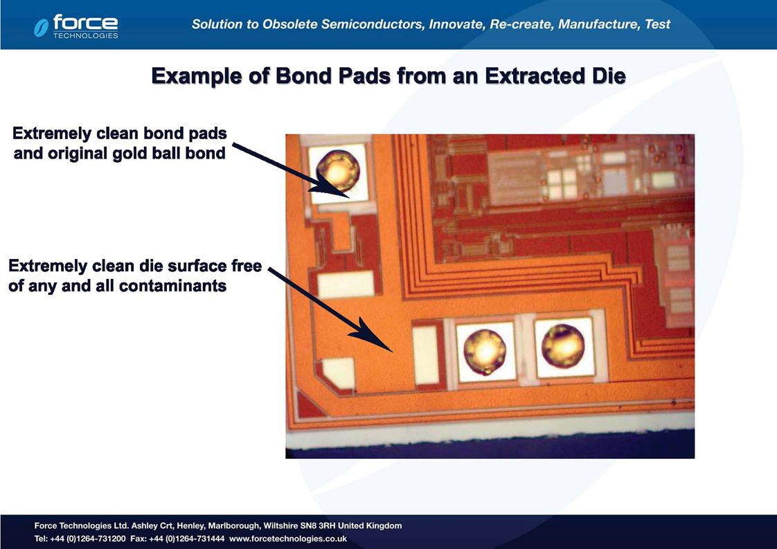
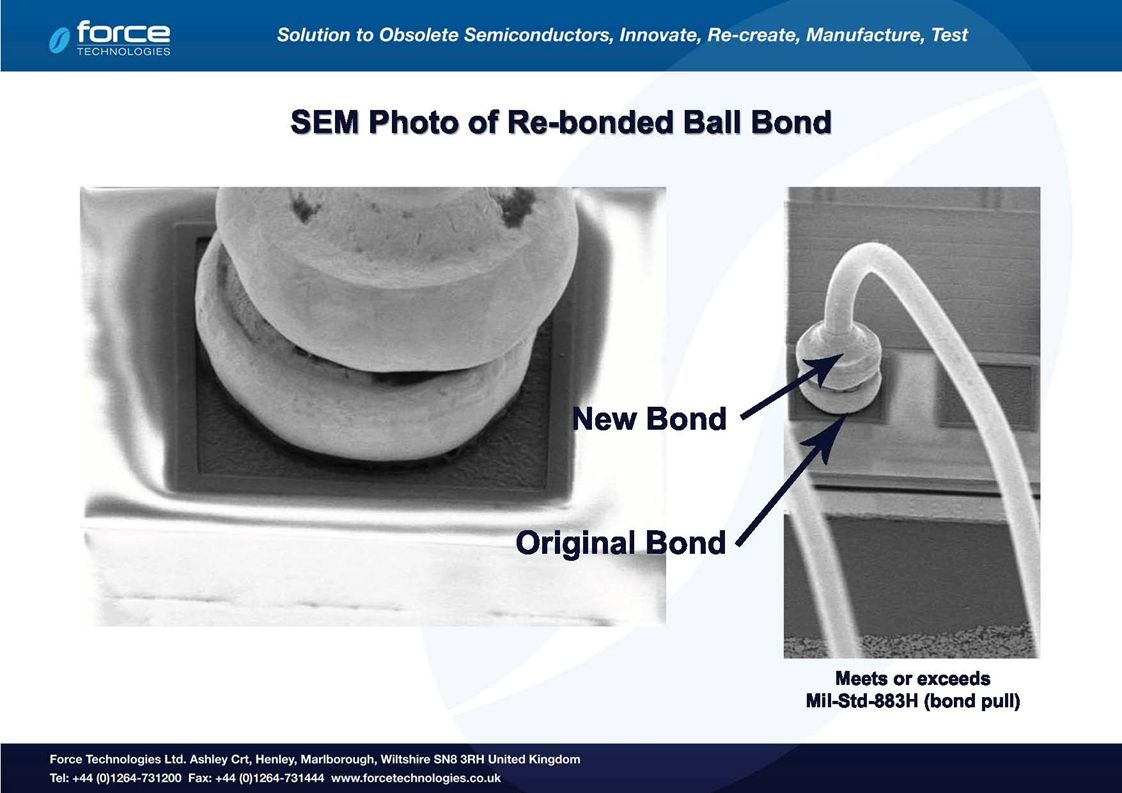
 products. For example, we have found that one particular popular plastic IC stopped functioning after only six (6) hours of unbiased exposure at 250C where the exact same die from the same wafer lot that has been removed from its plastic package and reassembled into a ceramic package using proprietary techniques will survive more than 1500 hours at 250C under identical conditions. This is a 250X multiple in product lifetime at 250C under identical conditions. Commercial ICs in plastic packages are generally manufactured to have 100year lifetimes at 50C under continuous operation. These lifetimes are extrapolated from accelerated life- tests performed generally at 125C (for 1000 hours) or at higher temperatures for exponentially shorter time periods according to the activation energy of the IC failure mechanisms of concern. This 250X increase in lifetime that we have achieved under identical conditions (250C) is highly significant given the fact that the die are identical between the original plastic package and the removed and reassembled die that was assembled into ceramic packages. The test conditions are, of course, also identical. The reason for this enormous disparity for the same die between ceramic and plastic packages is because the materials used in a plastic package greatly accelerates a failure mechanism that exponentially increases to quickly become the predominant IC failure mechanism at temperatures about 175C. Each of our customers performs their own internal qualification processes and qualify our products on a case by case basis. We have had no issues passing any qualification testing to which our products have been subjected and we fully expect that our products will experience the same level of success in each customer’s qualification testing. Question #6: The original IC would have been stress screened to accelerate visibility of process problems is this also true of your ICs. Response #6: Whatever stress screening has been performed on the original plastic IC would still be in effect when this die has been removed and re-assembled into another package. Question #7: The die extraction likely subjects the die to some aggressive chemicals and possible mechanical strain. Do we fully understand the effect of this on the 30 year expected life of the repackaged part as contamination cannot be 100% screened through visual inspections. Response #7: It is true that the chemicals used to remove the die from their plastic packages are fairly aggressive but these chemicals are no more aggressive than the chemicals to which these die were routinely exposed when they were originally processed in a wafer fabrication facility in their original wafer form. We also thoroughly clean the chemicals from the die following the die removal process. Following the die removal process, we end up with a pristine die that looks like a typical bare die with the exception that the original gold ball bonds are still present on the bond pads. Subsequent wire bonding is bonded to the original gold ball bond which has a very high capability that is equivalent to a gold ball bond on a virgin aluminium bond pad with the same distribution of bond pull strength. Adherence of gold to gold is extremely high. (See attached sample photos) We also routinely work with aluminium bond wire as well as is dictated to achieve the best available solution. We are extremely careful NOT to introduce mechanical strain to the die at any point through our process as this can cause micro cracking of polysilicon CMOS gates which would introduce an unwanted leakage and a potential latent reliability issue in an IC. Our die removal process is strictly a chemical process, not a mechanical process for this reason. Solution to Obsolete Semiconductors Innovate, Re-create, Manufacture, Test Force Technologies Ltd. Ashley Crt, Henley, Marlborough, Wiltshire SN8 3RH United Kingdom Tel: +44 (0) Fax: +44 (0)")
12
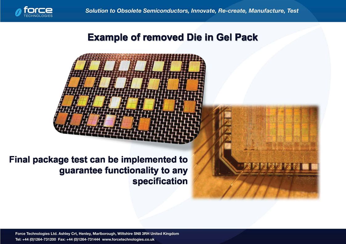
Frequently Asked Questions – FAQ Question #8: Do you have you any evidence of the results of subjecting a similar repackaged die to semiconductor industry standard accelerated aging effects testing? Response #8: Yes and we have passed all of this testing as well as or better than the original ICs have passed this testing. Question #10: What are the inspection and qualification processes? Response #10: 1) 100% Visual inspection and we screen for unclean parts and/or any cracking. 2) If we reassemble the die, we electrically test for continuity on all pins. Continuity testing involves test criteria for 'opens' and 'shorts'. Question #11: How do we assign a Part number on reassemble microelectronics? Question #11: How do we assign a Part number on reassemble microelectronics? Response #11: The original part number and manufacture is NOT Stamped on a reassembled package. A Unique part number is applied or a part number specified by the customer Question #12: How are the extracted die shipped Response #12: The die are placed in gel packs and vacuum is applied Solution to Obsolete Semiconductors Innovate, Re-create, Manufacture, Test Force Technologies Ltd. Ashley Crt, Henley, Marlborough, Wiltshire SN8 3RH United Kingdom Tel: +44 (0)1264-731200 Fax: +44 (0)1264-731444 www.forcetechnologies.co.uk
 100% Visual inspection and we screen for unclean parts and/or any cracking. 2) If we reassemble the die, we electrically test for continuity on all pins. Continuity testing involves test criteria for opens and shorts . Question #11: How do we assign a Part number on reassemble microelectronics. Question #11: How do we assign a Part number on reassemble microelectronics. Response #11: The original part number and manufacture is NOT Stamped on a reassembled package. A Unique part number is applied or a part number specified by the customer Question #12: How are the extracted die shipped Response #12: The die are placed in gel packs and vacuum is applied Solution to Obsolete Semiconductors Innovate, Re-create, Manufacture, Test Force Technologies Ltd. Ashley Crt, Henley, Marlborough, Wiltshire SN8 3RH United Kingdom Tel: +44 (0) Fax: +44 (0)")
Similar presentations


>")


 Non-Metals Sampling Procedures.>")

