Download presentation
Presentation is loading. Please wait.

1
STT read-out concepts Detectors requirements and layout Read-out concepts Developments of Analog FE and Digital Boards STS el. group : INFN, FZ Juelich, IFJ PAN, AGH Kraków, JU-Kraków discussed in Kraków meeting: 26/27.04. Grunberg 27-28.04

2
Central tracker : 4636 straws Forward tracker : ~13500 straws Drift time ~ 200 ns Time measurement: req. electronic resolution < 1 ns sensitivity (threshold) ~ 2 fC dE/dx, Q for PID : MIP: 5*10 6 e -, signal charge 10 6- 10 8 e - PID (Central tracker): 10% resolution in 24 layers detector capacitance: ~ 10-15 pF (9 pF/m) Hit rates up to 800 kHz/channel PANDA STT
 ~ 2 fC dE/dx, Q for PID : MIP: 5*10 6 e -, signal charge e - PID (Central tracker): 10% resolution in 24 layers detector capacitance: ~ pF (9 pF/m) Hit rates up to 800 kHz/channel PANDA STT.")
3
Expected rates p beam = 15 GeV/c, N Int =2x10 7 s -1. Forward STS Hit rate/cm/event in Central STS Max rate: ~ 5kHz/cm -> ~800 kHz for 150cm long tube Max rate: ~400 kHz for STS3 10 -3

4
Central Tracker

6
5-8 m

7
Forward tracker: 6 tracking stations: One tracking station with four double-layers Two double layers with vertical wires Two double layers with inclined wires e.g. (+10 ) and (-10 ) Two double layers with vertical wires prototype: Kraków
 and (-10 ) Two double layers with vertical wires prototype: Kraków.")
8
PANDA DAQ epoques (i.e 500 s)
")
9
Read-out concepts Complete read-out on detector avaliable space L <15 cm A<4000 cm 2 rad. hardness (FPGA’s in digital part!) cooling system needed Compact analog part on detector (ASIC rad. hard) (available space ~40 cm 2 for 16 channels) digital part (TDC/ADC) 5-8 m away outside detector nGbit/s links to Panda network at the moment considered as a base solution
 cooling system needed Compact analog part on detector (ASIC rad. hard) (available space ~40 cm 2 for 16 channels) digital part (TDC/ADC) 5-8 m away outside detector nGbit/s links to Panda network at the moment considered as a base solution.")
10
Developments concept based on TDC +(ADC?)-Kraków (AGH, JU) new dedicated analog ASIC (preamp+shaper+discriminator) TDC (HPTDC or in FPGA - new!) : TRB family TDC (GPX1 –HPTDC? ), ADC microTCA standard with PCe readout (Juelich) +10 GBit/s uplink module concept based on charge measurement in FADC ASIC : MSGCROC (AGH-Kraków) ADC + FPGA (Juelich) „ principle” evaluation: signal digitization (240 MHz FADC- from WASA) + analysis - Juelich
, ADC microTCA standard with PCe readout (Juelich) +10 GBit/s uplink module concept based on charge measurement in FADC ASIC : MSGCROC (AGH-Kraków) ADC + FPGA (Juelich) „ principle evaluation: signal digitization (240 MHz FADC- from WASA) + analysis - Juelich.")
11
Straw tubes read-out chain FE cards : Preamp+ Shaper+ BLR + Discriminator Dynamic Range ~ 5fC - 1pC, noise <1 fC Peaking time ~10-15 ns, Signal duration < 100 ns (pile-up < 10% @ 800 kHz) Gain 10-15 mV/fC Digital Boards Multihit TDC : Time measurement + TimeOverThreshold (TOT) for charge measurement OR/AND signal after shaper as input to FADC binning 0.5-0.8 ns Zero suppression & Hit detection.. Slow /Run/Data flow control Common Clock Distribution (i.e SODA) Data Concentration : gathering and sorting of hits marked by time stamps in epoques (i.e 500 s bunch) nGbit/s Optical serial link FE DB Panda DAQ - network
 Data Concentration : gathering and sorting of hits marked by time stamps in epoques (i.e 500 s bunch) nGbit/s Optical serial link FE DB Panda DAQ - network.")
12
CARIOCA 10 CARIOCA (IBM 0.25 m CMOS6SF ): 8 channels, preamp, shaper, BLR, discriminator, differential (LVDS) output: radiation hardness (checked for LHC requirements: no effects up to 20 Mrad dose) Sensitivity : at 220 pF for negative pulse : 7.7 mV/fC peaking time 14 ns, pulse width 60 ns power consumption ~40 mW/channel dev. at CERN for muon chambers no TOT ! - can be seen as back-up solution for Forward Tracker 4 ASIC FEE-UJ’2008

13
New ASIC for Panda STS Prototype I specification : submitted in April M. Idzik, D. Przyborowski AGH - Kraków not rad. hard BUT final version will be made in 0.125 m power consuption will go down by factor ~3

14
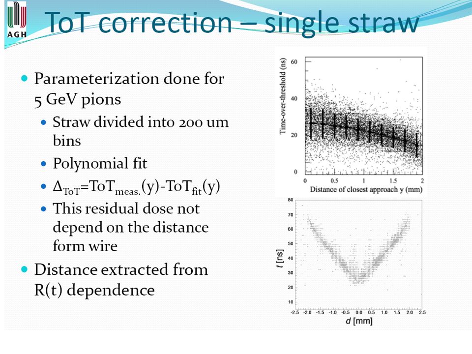
Characteristic : gain and linearity : straw signal from Garfield

15
Characteristic : TOT vs charge rec. range

16
TDC operation mode & data volume 1 MHz trigger clock (derived from SODA) : TDC with 0.5 ns binning: time 1 s range: 11 bits TOT 200 ns : 8 bits channel number(1-32): 5bits time stamp (i.e 1-500); 8 bits TDC id, +trailer/header ~ 5 bytes/hit Data volume: 32 channels TDC @ max 800 kHz hit rate/channel -> ~128 MB/s Data buffer : 32 channels TDC (i.e for 500 s epoque): 64-80 kB clock (1MHz) time measurement range T
 : TDC with 0.5 ns binning: time 1 s range: 11 bits TOT 200 ns : 8 bits channel number(1-32): 5bits time stamp (i.e 1-500); 8 bits TDC id, +trailer/header ~ 5 bytes/hit Data volume: 32 channels max 800 kHz hit rate/channel -> ~128 MB/s Data buffer : 32 channels TDC (i.e for 500 s epoque): kB clock (1MHz) time measurement range T")
17
step I (done): Trigger and Read-out Board TRB board developed by HADES DAQ group 2 versions alredy built many boards TRB v2 installed and used in the HADES DAQ 128 TDC channels (HPTDC) 130 MB/s data throughput achieved via optical links with TRBnet (8/10B in 2 Gbit/s) TRBnet protocol (FPGA): 3 logical channels; data transport, slow control, run control
: Trigger and Read-out Board TRB board developed by HADES DAQ group 2 versions alredy built many boards TRB v2 installed and used in the HADES DAQ 128 TDC channels (HPTDC) 130 MB/s data throughput achieved via optical links with TRBnet (8/10B in 2 Gbit/s) TRBnet protocol (FPGA): 3 logical channels; data transport, slow control, run control")
18
Marek Palka, GSI18 TRBv2 DC/DC ETRAX DSP FPGAVirtex4 TDC 0, 1 TDC 2, 3 SDRAM Optical link SDRAM Ethernet 128 TDC channels (100ps, 192ps, 780 ps) 2.5 Gb/s serial 8/10b link FPGA: TDC control + TrbNet Data flow control Slow control Run control
 2.5 Gb/s serial 8/10b link FPGA: TDC control + TrbNet Data flow control Slow control Run control")
19
STS test set-up (Kraków) TRB HUBCentral Trigger can connect up 16 TRB’s conversion to Gbit Ethernet -event building on PC used also in PANDA by DIRC groups : see docs on http://hades-wiki.gsi.de/cgi-bin/view/DaqSlowControl/TRBPublicationList
 TRB HUBCentral Trigger can connect up 16 TRB’s conversion to Gbit Ethernet -event building on PC used also in PANDA by DIRC groups : see docs on")
20
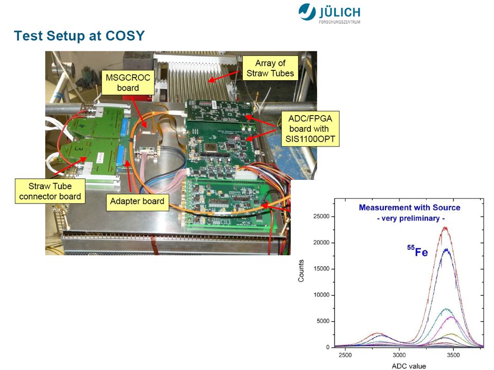
Some test results with Kraków- straws 32 channels – noise pattern Sr - source Drift time rise -10 ns range 180 ns

21
more powerfull: TRBv3 4 TDC in FPGA ( Lattice ECP3M) up to 40 TDC channels 4Mbit memory 1 FPGA for control (Run, Data, Slow- control) up to 8 x 3.2Gbit/s 8/10b serial links for data transmission: interface for Add-on connectors : i.e ADC ~ 20 W power See M. Traxler talk

22
not really tuned to STT range

23
Number of Boards/links CSTS: 4636 channels: ~ 145 x 32 channel TDC 145 x 3 Gbit/s links 37 TRB boards

25
also TDC based on GPX ASIC (8 channels and 81 ps resolution)
")
26
Developments in MTCA standard example: TDC board also board with ADC planned and 10 GB/s uplink module

27
Work packages detector –FEE connections/ cabling layout, connections to digital electronics - Juelich (CT), Kraków (FD) Analog FEE (time measurement, TOT +/or analog out)– AGH 1’st prototype submitted, test July/August Test with detector (time, TOT vs charge measurements) after freez-out of concept transmission to 0.125 MSGROC – future developments? ( discussion with AGH) TDC board based on TRB available, TRBv3 project started QDC boards in development in Juelich (MTCA). If TOT not satisfactory can be used for charge measurement
 TDC board based on TRB available, TRBv3 project started QDC boards in development in Juelich (MTCA). If TOT not satisfactory can be used for charge measurement.")
28
back-up

29
dE/dx simulation for STS

30
TOT– energy loss : HADES MDC dE/dx vs impact angle 24 * ~7 mm gaps He:Iso (2:1) FEE based on ASD8 chip measured: (J. Markert/ A.Schmah –U. Frankfurt)
.")
33
Time Over Threshold – energy loss resolution measured by HADES MDC

34
Test Setup 2 x TRBv2 1 x CTS Addon 1 x HUBv2 Addon 1 x CARIOCA 1 x Event building PC 1 x Optical switch XXXV PANDA Collaboration Workshop, GSI Darmstadt 30-11-2010 Grzegorz Korcyl – Jagiellonian University

35
Time resolution

36
Radiation dose: 1 year running time

Similar presentations

 CRYODET Workshop LNGS, 13-14 March 2006.>")


 GANDALF module TDC concepts TDC implementation in the FPGA measurements.>")


 T2K electronics Beam structure ~ 8 (9?) bunches / spill bunch width ~ 60 nsec bunch separation ~ 600 nsec spill duration ~ 5 sec Time between.>")


