Download presentation
Presentation is loading. Please wait.

1
Special Topics in Electronics Engineering
Spring 2014 RF Systems and Circuits Special Topics in Electronics Engineering Emad Hegazi Professor, ECE Communication Circuits Research Group

2
Spring 2014 RF Systems and Circuits Es/No or Eb/No=? 17!

3
Noise Figure Calculation
Spring 2014 RF Systems and Circuits Noise Figure Calculation RF input Baseband receiver 利用先前的公式可以計算出接收器的Noise Figure需要多小才能符合系統規格。

4
IP3 Calculation RF Systems and Circuits
Spring 2014 RF Systems and Circuits IP3 Calculation 利用系統規格的動態範圍以及所需的SNR可以計算出接收器的IP3規格。

5
Simplified Transceiver Architecture
Spring 2014 RF Systems and Circuits Simplified Transceiver Architecture In Hartley architecture, it translates the RF signal to IF signal by the different phase of the local oscillator, sinwt and coswt. Finally, the i-phase and the q-phase signal with 90 degree phase shifter are combined at the output. Thus the image signal has been suppressed.

6
Role of a Receiver RF Systems and Circuits Power Supply
Spring 2014 RF Systems and Circuits Role of a Receiver 90 A D HPMX-2007 The lkhefw wlkhq wilehr wejklh wajkhrqwilu wae. esjlkh qwh wlh lihewrw wklhjr qlih qilh q q3wih q Power Supply uP/ DSP Low Noise Amplifier Mixer Oscillator Baseband Processor De-Modulator bias I Data Q Data 1. amplify received signal with min. added noise 2. shift to lower frequency (cost and/or performance) 3. LO for down conversion 4. discard carrier and recover data Information Antenna
 3. LO for down conversion. 4. discard carrier and recover data. Information. Antenna.")
7
Can we use a BPF for channel selection?
Spring 2014 RF Systems and Circuits Can we use a BPF for channel selection? The adjacent channels are always considered as interferers. These interferes could affect the reception of the signal. It is important to filter the unnecessary channels Example: It is desired to filter the alternate channel by 35 dB using an LC-BPF. Determine the quality factor of the tank. Solution: 𝑍 𝑠 = 𝑅𝐿𝑠 𝑅𝐿𝐶 𝑠 2 +𝐿𝑠+𝑅 𝑍 𝑠 𝑅 ≈ 1 1+2𝑗𝑄 ∆𝑓 𝑓 𝑜 𝑄=63,200 B. Razavi: RF Microelectronics, 2nd Edition Too large cannot be achieved M. El-Nozahi

8
Band Selection The BPF before the LNA is used as a band select filter
Spring 2014 RF Systems and Circuits Band Selection B. Razavi: RF Microelectronics, 2nd Edition Band Select filter f Desired Band The BPF before the LNA is used as a band select filter Specification is relaxed compared to the case where it is used as a channel select filter It has a constant frequency response and does not need to be tunable The BPF is implemented using: SAW technology for frequencies below 10 GHZ MEMS technology for mm-wave frequencies M. El-Nozahi

9
Spring 2014 RF Systems and Circuits Band Selection B. Razavi: RF Microelectronics, 2nd Edition TX-RX feedthrough can limit the performance of the receiver Typically the received signal is in the order of -70 dBm Feedthrough may saturate the BB blocks because of the high gain Is an issue in full duplex transceivers Design Targets: LNA must tolerate this high input level A BPF is usually included at the output of LNA provide additional filtering M. El-Nozahi

10
Spring 2014 RF Systems and Circuits Band Selection B. Razavi: RF Microelectronics, 2nd Edition Band select filters are usually implemented in a duplexer Single antenna transceivers use a duplexer to isolate between TX and RX Duplexers are two BPF, one for RX and the other for TX M. El-Nozahi

11
Channel Selection Remarks
Spring 2014 RF Systems and Circuits Channel Selection Remarks Channel selection cannot be done before the LNA because: It is hard to find a BPF with large quality factor, and achieving a very small loss Having a tunable BPF with high quality factor is hard to obtained Usually, there are two steps to select a channel: Band selection: In which the entire band is selected. This step usually comes before the LNA. Channel selection: In which the desired channel is selected. This step is usually done after the first mixer. M. El-Nozahi

12
Superheterodyne Receiver
Spring 2014 RF Systems and Circuits Superheterodyne Receiver

13
Example: AM Radio AM radio band: 530 to 1610 KHz
Spring 2014 RF Systems and Circuits Example: AM Radio AM radio band: 530 to 1610 KHz BW/2 = ( )/2=1080/2=540, in band IF has to be lower. Commonly: 455kHz Image can be in AM band If LO is on low side, LO tuning range is: (530 to 1610) – 455 = (75 to 1155) LO lowest to highest is a factor of 15.4 If LO is on high side, LO tuning range is: (530 to 1610) = (985 to 2065) LO lowest to highest is a factor of 2.01
/2=1080/2=540, in band. IF has to be lower. Commonly: 455kHz. Image can be in AM band. If LO is on low side, LO tuning range is: (530 to 1610) – 455 = (75 to 1155) LO lowest to highest is a factor of If LO is on high side, LO tuning range is: (530 to 1610) = (985 to 2065) LO lowest to highest is a factor of")
14
Typical Superheterodyne Digital Receiver
Spring 2014 RF Systems and Circuits Typical Superheterodyne Digital Receiver Prof. E Sanchez-Sinencio RF course slides Advantage Disadvantages Good selectivity High complexity Good sensitivity High power consumption Image problem External components Not suitable for multi-standard

15
The Image Problem The image could be another user or standard
Spring 2014 RF Systems and Circuits The Image Problem Prof. E Sanchez-Sinencio RF course slides The image could be another user or standard The image must be filtered out before going the mixer Frequency planning is key

16
Image Rejection Calculation
Spring 2014 RF Systems and Circuits Image Rejection Calculation PImage IRrequired Pdesired SNRmin 決定了中頻之後,依據系統的規格可以計算出鏡像消除的規格。 fIF fRF fLO (all in dB’s)
")
17
Mixer = Multiplying up/down conversion
Spring 2014 RF Systems and Circuits Mixer = Multiplying up/down conversion Frequency translation device Ideal mixer: Doesn’t “mix”; it multiplies AB A B

18
Super-heterodyne Receiver
Spring 2014 RF Systems and Circuits Super-heterodyne Receiver In Hartley architecture, it translates the RF signal to IF signal by the different phase of the local oscillator, sinwt and coswt. Finally, the i-phase and the q-phase signal with 90 degree phase shifter are combined at the output. Thus the image signal has been suppressed.

19
Selection of IF If IF is large, Other IF selection criteria
Spring 2014 RF Systems and Circuits Selection of IF If IF is large, better separation between RF and image better image rejection easier image rejection filter design More stages of down conversion Other IF selection criteria Select IF so that image freq is outside of RF band IF >= (RF BW)/2 Sometime may not be possible, if (RF BW)/2 is within RF Band
/2. Sometime may not be possible, if (RF BW)/2 is within RF Band.")
20
Q: should LO > RF, or LO < RF??
Spring 2014 RF Systems and Circuits For each channel assignment, there are two choices of LO freq that meets the requirement |RF–LO|=IF. Q: should LO > RF, or LO < RF??

21
Image problem converting to IF
Spring 2014 RF Systems and Circuits Image problem converting to IF A has desired signal at wIF A1cos(wRFt) plus an interference at wIM A2cos(wIMt) B is at wLO And: In Hartley architecture, it translates the RF signal to IF signal by the different phase of the local oscillator, sinwt and coswt. Finally, the i-phase and the q-phase signal with 90 degree phase shifter are combined at the output. Thus the image signal has been suppressed. wRF - wLO = wLO - wIM = wIF Both converted to IF, Can’t be cleaned once corrupted
 plus an interference at wIM. A2cos(wIMt) B is at wLO. And: In Hartley architecture, it translates the RF signal to IF signal by the different phase of the local oscillator, sinwt and coswt. Finally, the i-phase and the q-phase signal with 90 degree phase shifter are combined at the output. Thus the image signal has been suppressed. wRF - wLO = wLO - wIM = wIF. Both converted to IF, Can’t be cleaned once corrupted.")
22
Spring 2014 RF Systems and Circuits Image Problem

23
Problem of Image Signal
Spring 2014 RF Systems and Circuits Problem of Image Signal

24
Problem of Image Signal
Spring 2014 RF Systems and Circuits Problem of Image Signal Solution: Image Rejection Filter

25
The Image Problem Image Reject filter versus channel selection:
Spring 2014 RF Systems and Circuits The Image Problem Image Reject filter versus channel selection: Larger IF frequencies requires channel select filter with higher Q B. Razavi: RF Microelectronics, 2nd Edition M. El-Nozahi

26
Dual-IF Heterodyne Receiver
Spring 2014 RF Systems and Circuits Dual-IF Heterodyne Receiver Channel selection is done in two stages, hence relaxing the specification for each stage Secondary image problem To avoid the problem, the second IF frequency is set to zero Is it possible to have a zero IF? M. El-Nozahi

27
Down Conversion to IF AM modulation: RF Systems and Circuits
Spring 2014 RF Systems and Circuits Down Conversion to IF AM modulation: FM/ Digital ..etc . modulations: M. El-Nozahi

28
High Q Alternatives What is really needed is not really a filter.
Spring 2014 RF Systems and Circuits High Q Alternatives What is really needed is not really a filter. A cancellation scheme to reject noise is good enough Cosine wave

29
High Q Alternatives What if we use a sine wave instead
Spring 2014 RF Systems and Circuits High Q Alternatives What if we use a sine wave instead j j -j -j

30
Complex Signal Representation
Spring 2014 RF Systems and Circuits Complex Signal Representation Niknejad and Shana’a

31
Orthogonality of I and Q
Spring 2014 RF Systems and Circuits Orthogonality of I and Q Niknejad and Shana’a

32
Orthogonality Design of RF Circuits & Systems RF Systems and Circuits
Spring 2014 RF Systems and Circuits Orthogonality Spring 2014 Design of RF Circuits & Systems

33
Image Reject Receivers-I
Spring 2014 RF Systems and Circuits Image Reject Receivers-I What is a shift by 90o? 𝐴 cos 𝜔 𝑐 𝑡−90 =−𝑗 𝐴 2 𝑒 𝑗 𝜔 𝑐 𝑡 +𝑗 𝐴 2 𝑒 −𝑗 𝜔 𝑐 𝑡 The 90o phase shift is also called Hilbert transform Im Im 𝑗 𝐴 2 Re Re 𝐴 2 𝐴 2 fc f -fc fc f -fc −𝑗 𝐴 2 𝑋90(𝜔)=𝑋(𝜔) −𝑗 𝑠𝑔𝑛(𝜔) M. El-Nozahi
=𝑋(𝜔) −𝑗 𝑠𝑔𝑛(𝜔) M. El-Nozahi.")
34
Hilbert transform: A 90o phase shift results in:
Spring 2014 RF Systems and Circuits Hilbert transform: A 90o phase shift results in: Rotating positive frequency components CW by 90o Rotating negative frequency components CCW by 90o Multiplication by +j rotates all frequency components CCW by 90o. Multiplication by -j rotates all frequency components CW by 90o. Note that for DC frequencies these transformations do not have any meaning M. El-Nozahi

35
Spring 2014 RF Systems and Circuits Hilbert transform Assume I(t) is shifted by 90o to produce Q(t). Find I(t)+jQ(t). f fc -fc Re{I} Im{I} f fc -fc Re{Q} Im{Q} f fc -fc Re{jQ} Im{jQ} Im{I+jQ} f fc -fc Re{I+jQ} M. El-Nozahi

36
Image Reject Receivers
Spring 2014 RF Systems and Circuits Image Reject Receivers Idea: From the previous example it seems that one could remove the image with the help of quadrature components. Im{I}} Re{I} Im{I} Re{I} f -fIF fIF Im{Q} Re{Q} f -fs -fi fi fs fLO f -fIF fIF M. El-Nozahi

37
Hartley Image Reject Architecture
Spring 2014 RF Systems and Circuits Hartley Image Reject Architecture B. Razavi: RF Microelectronics, 2nd Edition A Hilbert transform is used to cancel the image I&Q (quadrature) signals are generated for image rejection. The generation of the 90o could be achieved using RC phase shifter each providing 45o phase shift (narrow band solution) M. El-Nozahi
 signals are generated for image rejection. The generation of the 90o could be achieved using RC phase. shifter each providing 45o phase shift (narrow band solution) M. El-Nozahi.")
38
Hartley Image Reject Architecture
Spring 2014 RF Systems and Circuits Hartley Image Reject Architecture B. Razavi: RF Microelectronics, 2nd Edition Still in the BB we must generate another I&Q for digital demodulation Drawbacks: Mismatch between the two path will result in finite image rejection The RC solution can be used for narrow-band architectures. Wideband architecture will result in degraded performance for the image rejection (IRR) Typical values for IRR is lower than 35 dB. M. El-Nozahi
 Typical values for IRR is lower than 35 dB. M. El-Nozahi.")
39
Implementing the Phase Shift
Spring 2014 RF Systems and Circuits Implementing the Phase Shift Hartley Architecture with simple 90 deg phase shiftor

43
RF Systems and Circuits
Spring 2014 RF Systems and Circuits

44
IRR

45
Input image power ratio

46
Gain Mismatch due to R, C errors
Spring 2014 RF Systems and Circuits Gain Mismatch due to R, C errors At w = 1/RC:

47
Weaver Image Reject Architecture
Spring 2014 RF Systems and Circuits Weaver Image Reject Architecture Hilbert transform is obtained using another quadrature (complex) mixing stage Advantages compared to Hartley: Better accuracy in generating the additional 90o phase shift IRR is limited to 40 dB, which is higher than Hartley architecture Disadvantages: Secondary image problem B. Razavi: RF Microelectronics, 2nd Edition M. El-Nozahi
 mixing stage. Advantages compared to Hartley: Better accuracy in generating the additional 90o phase shift. IRR is limited to 40 dB, which is higher than Hartley architecture. Disadvantages: Secondary image problem. B. Razavi: RF Microelectronics, 2nd Edition. M. El-Nozahi.")
48
Direct Conversion Receiver
Spring 2014 RF Systems and Circuits Direct Conversion Receiver A single step down conversion is used. The output frequency is at DC B. Razavi: RF Microelectronics, 2nd Edition Advantages Disadvantages No image problem LO leakage Less complex / low power consumption DC offset Channel selection is done with a LPF Even order distortion Effect of mixer spurs are reduced Flicker noise IQ mismatch M. El-Nozahi

49
Spring 2014 RF Systems and Circuits LO Leakage The LO signal can be leaked to the antenna by the capacitive coupling or substrate For singled ended Los, the LO leakage can reach -60 dBm Differential LO architectures have lower LO leakage (better than dBm) B. Razavi: RF Microelectronics, 2nd Edition M. El-Nozahi
 B. Razavi: RF Microelectronics, 2nd Edition. M. El-Nozahi.")
50
Direct Conversion Receiver
Spring 2014 RF Systems and Circuits Direct Conversion Receiver DC Offset: The leaked LO signal can go through the antenna, LNA and down converted Because of the LO signal and its feedthrough signal carry the same frequency, a DC offset is produced (this phenomena is called LO self mixing). BB blocks usually have high again, hence the LO self mixing may saturate the receiver HPF are not common because they require a very low cut-off frequency (large components, slow settling) B. Razavi: RF Microelectronics, 2nd Edition M. El-Nozahi
. BB blocks usually have high again, hence the LO self mixing may saturate. the receiver. HPF are not common because they require a very low cut-off frequency (large components, slow settling) B. Razavi: RF Microelectronics, 2nd Edition. M. El-Nozahi.")
51
Even Order Distortion RF Systems and Circuits
Spring 2014 RF Systems and Circuits Even Order Distortion B. Razavi: RF Microelectronics, 2nd Edition M. El-Nozahi

52
Direct Conversion Receiver
Spring 2014 RF Systems and Circuits Direct Conversion Receiver Flicker Noise: For g the channel bandwidth is 10MHz. With a noise corner frequency of 200kHz For GSM, the channel bandwidth is 100 kHz and therefore a large portion of noise appears due to flicker noise B. Razavi: RF Microelectronics, 2nd Edition M. El-Nozahi

53
Direct Conversion Receiver
Spring 2014 RF Systems and Circuits Direct Conversion Receiver IQ mismatch: mismatch in I and Q path affects SNR of received signals Mismatch effects are more dominate at high frequencies. Reducing the frequency at which the I and Q signal are generated enhances the SNR Digital calibration is used to correct these mismatches Amplitude mismatch: Phase mismatch: M. El-Nozahi

54
Low-IF Receiver Has all the advantages of direct conversion receivers
Spring 2014 RF Systems and Circuits Low-IF Receiver Has all the advantages of direct conversion receivers More difficult image rejection requirements Minimum IF frequency is channel bandwidth DC offset is outside the signal bandwidth Complex Filter Large Requires matching Power hungry

55
Low IF receiver - Quadrature RF down conversion required
Spring 2014 RF Systems and Circuits Low IF receiver + Eliminate IF SAW, IF PLL and image filtering + Integration + Relaxes image rejection requirements + Avoids DC problems, relaxes 1/f noise problem - Quadrature RF down conversion required - Require higher performance ADC Additional mixer Slower RF PLL settling Even order distortion still problem Low freq IF filters require large chip area

56
Low-IF Down Conversion
Spring 2014 RF Systems and Circuits Low-IF Down Conversion Complex BPF Mirror signal, needs removal

57
Mirror Signal Suppression
Spring 2014 RF Systems and Circuits Mirror Signal Suppression Complex Bandpass Filter I Q I Q LO1 LO2

58
Complex Mixing- Real LO
Spring 2014 RF Systems and Circuits Complex Mixing- Real LO

59
Complex Mixing-Complex LO
Spring 2014 RF Systems and Circuits Complex Mixing-Complex LO

60
Spring 2014 RF Systems and Circuits Complex Mixing

61
Spring 2014 RF Systems and Circuits Bluetooth Receiver Has all the advantages of direct conversion receivers More difficult image rejection requirements Minimum IF frequency is channel bandwidth DC offset is outside the signal bandwidth

62
Direct Conversion Receiver
Spring 2014 RF Systems and Circuits Direct Conversion Receiver In Hartley architecture, it translates the RF signal to IF signal by the different phase of the local oscillator, sinwt and coswt. Finally, the i-phase and the q-phase signal with 90 degree phase shifter are combined at the output. Thus the image signal has been suppressed. Little image problem No IQ IF

63
Direct Conversion Receiver
Spring 2014 RF Systems and Circuits Direct Conversion Receiver LO is at same frequency as RF 1/f noise here can end up in channel Self mixing cause DC problem - Quadrature RF down conversion required - DC problem - Typically requires offset or 2x LO to avoid coupling + Eliminate IF SAW, IF PLL and image filtering + Integration + easier image problem

64
DC Offset (Self-mixing)
Spring 2014 RF Systems and Circuits DC Offset (Self-mixing) A D w c aLO(t)=ALOcos(w c+q) capacitive coupling substrate coupling bondwire coupling Saturates the following stages A D w c
 A. D. w c. aLO(t)=ALOcos(w c+q) capacitive coupling. substrate coupling. bondwire coupling. Saturates the following stages. A. D. w c.")
65
DC Offset (Self-mixing)
Spring 2014 RF Systems and Circuits DC Offset (Self-mixing) level DC Offset + - t
 level. DC Offset. + - t.")
66
DC Offset Cancellation
Spring 2014 RF Systems and Circuits DC Offset Cancellation Capacitive Coupling Requires a large capacitor Negative Feedback Nonlinear -A

67
Spring 2014 RF Systems and Circuits 1/f noise effect CMOS transistors has significant 1/f noise at low to DC frequency Significantly noise performance of direct conversion receivers Receive signal 1/f noise f

68
Even-Order Distortion
Spring 2014 RF Systems and Circuits Even-Order Distortion Interferers Dw y(t) = a1 x(t) + a2 x2(t) a2 A1A2 cos(Dw) Direct feed through Dw Direct feed through
 = a1 x(t) + a2 x2(t) a2 A1A2 cos(Dw) Direct feed through. Dw. Direct feed through.")
69
Mirror Signal Upper sideband and lower sideband are identical
Spring 2014 RF Systems and Circuits Mirror Signal Upper sideband and lower sideband are identical

70
Mirror Signal Upper sideband and lower sideband are not identical
Spring 2014 RF Systems and Circuits Mirror Signal Upper sideband and lower sideband are not identical

71
Mirror Signal Suppression
Spring 2014 RF Systems and Circuits Mirror Signal Suppression Quadrature Down Conversion A D 90 a(t) ui(t) uq(t) vi(t) vq(t) I Q
 ui(t) uq(t) vi(t) vq(t) I. Q.")
72
Quadrature Conversion
Spring 2014 RF Systems and Circuits Quadrature Conversion

73
Quadrature Down Conversion
Spring 2014 RF Systems and Circuits Quadrature Down Conversion

74
I/Q Mismatch RF Systems and Circuits I Phase & Gain Error a(t) Q 90
Spring 2014 RF Systems and Circuits I/Q Mismatch 90 I Q Phase & Gain Error a(t)
")
75
I/Q Mismatch due to LO errors
Spring 2014 RF Systems and Circuits I/Q Mismatch due to LO errors

76
RF Systems and Circuits
Spring 2014 RF Systems and Circuits

77
RF Systems and Circuits
Spring 2014 RF Systems and Circuits Use of I/Q down conversion recovers the nonsymmetrical receive signal spectrum But port isolation becomes more challenging Selfmixing and even order distortion may affect both channels and affect each other, causing additional I/Q mismatch

78
RF Systems and Circuits
Spring 2014 RF Systems and Circuits 90 a(t) A/D Base Band DSP Phase and gain mismatch compensation DC and 1/f cancellation
 A/D. Base. Band. DSP. Phase and gain mismatch. compensation. DC and 1/f. cancellation.")
79
Summary of Direct Conversion Receiver
Spring 2014 RF Systems and Circuits Summary of Direct Conversion Receiver No need for imager reject filter Suitable for monolithic integration with baseband DC offsets due to crosstalk of input ports of mixer Even order IM direct feed through to baseband Quadrature down conversion suppresses mirror I/Q mismatch due to mismatches in parasitics Low power consumption attributes to less hardware

80
Spring 2014 RF Systems and Circuits Balun Texas Instruments 2006

81
Spring 2014 RF Systems and Circuits Phase Noise Texas Instruments 2006

82
Trsnmitter Paradigms Signal is strong.
Spring 2014 RF Systems and Circuits Trsnmitter Paradigms Signal is strong. We need to make sure efficient delivery of power to the antenna. Spectral content should be contained to its specified limits. Linearity matters if modulation is linear. 傳送器的結構有直接升頻與二次升頻結構。

83
Transmit Specifications
Spring 2014 RF Systems and Circuits Transmit Specifications Transmit spectrum mask

84
Transmitter Specifications
Spring 2014 RF Systems and Circuits Transmitter Specifications alternate adjacent channel Adjacent channel 20 20 40 40

85
Transmitter Architectures
Spring 2014 RF Systems and Circuits Transmitter Architectures Direct Conversion Transmitter Two-step Conversion Transmitter Offset PLL Transmitter 傳送器的結構有直接升頻與二次升頻結構。

86
Direct-conversion transmitter
Spring 2014 RF Systems and Circuits Direct-conversion transmitter I 90 Q 直接升頻的缺點是LO的信號會透過天線發射出去。 wLO Pros: less spurious synthesized Cons: more LO pulling

87
Direct-conversion transmitter with offset LO
Spring 2014 RF Systems and Circuits Direct-conversion transmitter with offset LO I wLO 90 w1 Q w2 Pros: less LO pulling Cons: more spurious synthesized

88
Two-step transmitter RF Systems and Circuits I w1+w2 cosw1t cosw2t Q
Spring 2014 RF Systems and Circuits Two-step transmitter I 90 w1+w2 cosw1t cosw2t Q 二次升頻則先升至中頻,再往上升頻至所要的頻率,是較常見的結構。 Pros: less LO pulling superior IQ matching Cons: required high-Q bandpass filter

89
Offset PLL Transmitter
Spring 2014 RF Systems and Circuits Offset PLL Transmitter I PD/LPF VCO 90 cosw1t Q 1/N

90
Simplified Transceiver Architecture
Spring 2014 RF Systems and Circuits Simplified Transceiver Architecture In Hartley architecture, it translates the RF signal to IF signal by the different phase of the local oscillator, sinwt and coswt. Finally, the i-phase and the q-phase signal with 90 degree phase shifter are combined at the output. Thus the image signal has been suppressed.

91
Role of a Receiver RF Systems and Circuits Power Supply
Spring 2014 RF Systems and Circuits Role of a Receiver 90 A D HPMX-2007 The lkhefw wlkhq wilehr wejklh wajkhrqwilu wae. esjlkh qwh wlh lihewrw wklhjr qlih qilh q q3wih q Power Supply uP/ DSP Low Noise Amplifier Mixer Oscillator Baseband Processor De-Modulator bias I Data Q Data 1. amplify received signal with min. added noise 2. shift to lower frequency (cost and/or performance) 3. LO for down conversion 4. discard carrier and recover data Information Antenna
 3. LO for down conversion. 4. discard carrier and recover data. Information. Antenna.")
92
Can we use a BPF for channel selection?
Spring 2014 RF Systems and Circuits Can we use a BPF for channel selection? The adjacent channels are always considered as interferers. These interferes could affect the reception of the signal. It is important to filter the unnecessary channels Example: It is desired to filter the alternate channel by 35 dB using an LC-BPF. Determine the quality factor of the tank. Solution: 𝑍 𝑠 = 𝑅𝐿𝑠 𝑅𝐿𝐶 𝑠 2 +𝐿𝑠+𝑅 𝑍 𝑠 𝑅 ≈ 1 1+2𝑗𝑄 ∆𝑓 𝑓 𝑜 𝑄=63,200 B. Razavi: RF Microelectronics, 2nd Edition Too large cannot be achieved

93
Band Selection The BPF before the LNA is used as a band select filter
Spring 2014 RF Systems and Circuits Band Selection B. Razavi: RF Microelectronics, 2nd Edition Band Select filter f Desired Band The BPF before the LNA is used as a band select filter Specification is relaxed compared to the case where it is used as a channel select filter It has a constant frequency response and does not need to be tunable The BPF is implemented using: SAW technology for frequencies below 10 GHZ MEMS technology for mm-wave frequencies

94
Spring 2014 RF Systems and Circuits Band Selection B. Razavi: RF Microelectronics, 2nd Edition TX-RX feedthrough can limit the performance of the receiver Typically the received signal is in the order of -70 dBm Feedthrough may saturate the BB blocks because of the high gain Is an issue in full duplex transceivers Design Targets: LNA must tolerate this high input level A BPF is usually included at the output of LNA provide additional filtering

95
Spring 2014 RF Systems and Circuits Band Selection B. Razavi: RF Microelectronics, 2nd Edition Band select filters are usually implemented in a duplexer Single antenna transceivers use a duplexer to isolate between TX and RX Duplexers are two BPF, one for RX and the other for TX

96
Channel Selection Remarks
Spring 2014 RF Systems and Circuits Channel Selection Remarks Channel selection cannot be done before the LNA because: It is hard to find a BPF with large quality factor, and achieving a very small loss Having a tunable BPF with high quality factor is hard to obtained Usually, there are two steps to select a channel: Band selection: In which the entire band is selected. This step usually comes before the LNA. Channel selection: In which the desired channel is selected. This step is usually done after the first mixer.

97
Superheterodyne Receiver
Spring 2014 RF Systems and Circuits Superheterodyne Receiver

98
Example: AM Radio AM radio band: 530 to 1610 KHz
Spring 2014 RF Systems and Circuits Example: AM Radio AM radio band: 530 to 1610 KHz BW/2 = ( )/2=1080/2=540, in band IF has to be lower. Commonly: 455kHz Image can be in AM band If LO is on low side, LO tuning range is: (530 to 1610) – 455 = (75 to 1155) LO lowest to highest is a factor of 15.4 If LO is on high side, LO tuning range is: (530 to 1610) = (985 to 2065) LO lowest to highest is a factor of 2.01
/2=1080/2=540, in band. IF has to be lower. Commonly: 455kHz. Image can be in AM band. If LO is on low side, LO tuning range is: (530 to 1610) – 455 = (75 to 1155) LO lowest to highest is a factor of If LO is on high side, LO tuning range is: (530 to 1610) = (985 to 2065) LO lowest to highest is a factor of")
99
Typical Superheterodyne Digital Receiver
Spring 2014 RF Systems and Circuits Typical Superheterodyne Digital Receiver Prof. E Sanchez-Sinencio RF course slides Advantage Disadvantages Good selectivity High complexity Good sensitivity High power consumption Image problem External components Not suitable for multi-standard

100
The Image Problem The image could be another user or standard
Spring 2014 RF Systems and Circuits The Image Problem Prof. E Sanchez-Sinencio RF course slides The image could be another user or standard The image must be filtered out before going the mixer Frequency planning is key

101
Image Rejection Calculation
Spring 2014 RF Systems and Circuits Image Rejection Calculation PImage IRrequired Pdesired SNRmin 決定了中頻之後,依據系統的規格可以計算出鏡像消除的規格。 fIF fRF fLO (all in dB’s)
")
102
Mixer = Multiplying up/down conversion
Spring 2014 RF Systems and Circuits Mixer = Multiplying up/down conversion Frequency translation device Ideal mixer: Doesn’t “mix”; it multiplies AB A B

103
Super-heterodyne Receiver
Spring 2014 RF Systems and Circuits Super-heterodyne Receiver In Hartley architecture, it translates the RF signal to IF signal by the different phase of the local oscillator, sinwt and coswt. Finally, the i-phase and the q-phase signal with 90 degree phase shifter are combined at the output. Thus the image signal has been suppressed.

104
Selection of IF If IF is large, Other IF selection criteria
Spring 2014 RF Systems and Circuits Selection of IF If IF is large, better separation between RF and image better image rejection easier image rejection filter design More stages of down conversion Other IF selection criteria Select IF so that image freq is outside of RF band IF >= (RF BW)/2 Sometime may not be possible, if (RF BW)/2 is within RF Band
/2. Sometime may not be possible, if (RF BW)/2 is within RF Band.")
105
Q: should LO > RF, or LO < RF??
Spring 2014 RF Systems and Circuits For each channel assignment, there are two choices of LO freq that meets the requirement |RF–LO|=IF. Q: should LO > RF, or LO < RF??

106
Image problem converting to IF
Spring 2014 RF Systems and Circuits Image problem converting to IF A has desired signal at wIF A1cos(wRFt) plus an interference at wIM A2cos(wIMt) B is at wLO And: In Hartley architecture, it translates the RF signal to IF signal by the different phase of the local oscillator, sinwt and coswt. Finally, the i-phase and the q-phase signal with 90 degree phase shifter are combined at the output. Thus the image signal has been suppressed. wRF - wLO = wLO - wIM = wIF Both converted to IF, Can’t be cleaned once corrupted
 plus an interference at wIM. A2cos(wIMt) B is at wLO. And: In Hartley architecture, it translates the RF signal to IF signal by the different phase of the local oscillator, sinwt and coswt. Finally, the i-phase and the q-phase signal with 90 degree phase shifter are combined at the output. Thus the image signal has been suppressed. wRF - wLO = wLO - wIM = wIF. Both converted to IF, Can’t be cleaned once corrupted.")
107
Spring 2014 RF Systems and Circuits Image Problem

108
Problem of Image Signal
Spring 2014 RF Systems and Circuits Problem of Image Signal

109
Problem of Image Signal
Spring 2014 RF Systems and Circuits Problem of Image Signal Solution: Image Rejection Filter

110
The Image Problem Image Reject filter versus channel selection:
Spring 2014 RF Systems and Circuits The Image Problem Image Reject filter versus channel selection: Larger IF frequencies requires channel select filter with higher Q B. Razavi: RF Microelectronics, 2nd Edition

111
Dual-IF Heterodyne Receiver
Spring 2014 RF Systems and Circuits Dual-IF Heterodyne Receiver Channel selection is done in two stages, hence relaxing the specification for each stage Secondary image problem To avoid the problem, the second IF frequency is set to zero Is it possible to have a zero IF?

112
Down Conversion to IF AM modulation: RF Systems and Circuits
Spring 2014 RF Systems and Circuits Down Conversion to IF AM modulation: FM/ Digital ..etc . modulations:

113
High Q Alternatives What is really needed is not really a filter.
Spring 2014 RF Systems and Circuits High Q Alternatives What is really needed is not really a filter. A cancellation scheme to reject noise is good enough Cosine wave

114
High Q Alternatives What if we use a sine wave instead
Spring 2014 RF Systems and Circuits High Q Alternatives What if we use a sine wave instead

115
Complex Signal Representation
Spring 2014 RF Systems and Circuits Complex Signal Representation Niknejad and Shana’a

116
Orthognality of I and Q RF Systems and Circuits Niknejad and Shana’a
Spring 2014 RF Systems and Circuits Orthognality of I and Q Niknejad and Shana’a

117
Orthogonality Design of RF Circuits & Systems RF Systems and Circuits
Spring 2014 RF Systems and Circuits Orthogonality Spring 2014 Design of RF Circuits & Systems

118
Image Reject Receivers-I
Spring 2014 RF Systems and Circuits Image Reject Receivers-I What is a shift by 90o? 𝐴 cos 𝜔 𝑐 𝑡−90 =−𝑗 𝐴 2 𝑒 𝑗 𝜔 𝑐 𝑡 +𝑗 𝐴 2 𝑒 −𝑗 𝜔 𝑐 𝑡 The 90o phase shift is also called Hilbert transform Im Im 𝑗 𝐴 2 Re Re 𝐴 2 𝐴 2 fc f -fc fc f -fc −𝑗 𝐴 2 𝑋90(𝜔)=𝑋(𝜔) −𝑗 𝑠𝑔𝑛(𝜔)
=𝑋(𝜔) −𝑗 𝑠𝑔𝑛(𝜔)")
119
Hilbert transform: A 90o phase shift results in:
Spring 2014 RF Systems and Circuits Hilbert transform: A 90o phase shift results in: Rotating positive frequency components CW by 90o Rotating negative frequency components CCW by 90o Multiplication by +j rotates all frequency components CCW by 90o. Multiplication by -j rotates all frequency components CW by 90o. Note that for DC frequencies these transformations do not have any meaning

120
Spring 2014 RF Systems and Circuits Hilbert transform Assume I(t) is shifted by 90o to produce Q(t). Find I(t)+jQ(t). f fc -fc Re{I} Im{I} f fc -fc Re{Q} Im{Q} f fc -fc Re{jQ} Im{jQ} Im{I+jQ} f fc -fc Re{I+jQ}

121
Image Reject Receivers
Spring 2014 RF Systems and Circuits Image Reject Receivers Idea: From the previous example it seems that one could remove the image with the help of quadrature components. Im{I}} Re{I} Im{I} Re{I} f -fIF fIF Im{Q} Re{Q} f -fs -fi fi fs fLO f -fIF fIF

122
Hartley Image Reject Architecture
Spring 2014 RF Systems and Circuits Hartley Image Reject Architecture B. Razavi: RF Microelectronics, 2nd Edition A Hilbert transform is used to cancel the image I&Q (quadrature) signals are generated for image rejection. The generation of the 90o could be achieved using RC phase shifter each providing 45o phase shift (narrow band solution)
 signals are generated for image rejection. The generation of the 90o could be achieved using RC phase. shifter each providing 45o phase shift (narrow band solution)")
123
Hartley Image Reject Architecture
Spring 2014 RF Systems and Circuits Hartley Image Reject Architecture B. Razavi: RF Microelectronics, 2nd Edition Still in the BB we must generate another I&Q for digital demodulation Drawbacks: Mismatch between the two path will result in finite image rejection The RC solution can be used for narrow-band architectures. Wideband architecture will result in degraded performance for the image rejection (IRR) Typical values for IRR is lower than 35 dB.
 Typical values for IRR is lower than 35 dB.")
124
Implementing the Phase Shift
Spring 2014 RF Systems and Circuits Implementing the Phase Shift Hartley Architecture with simple 90 deg phase shiftor

125
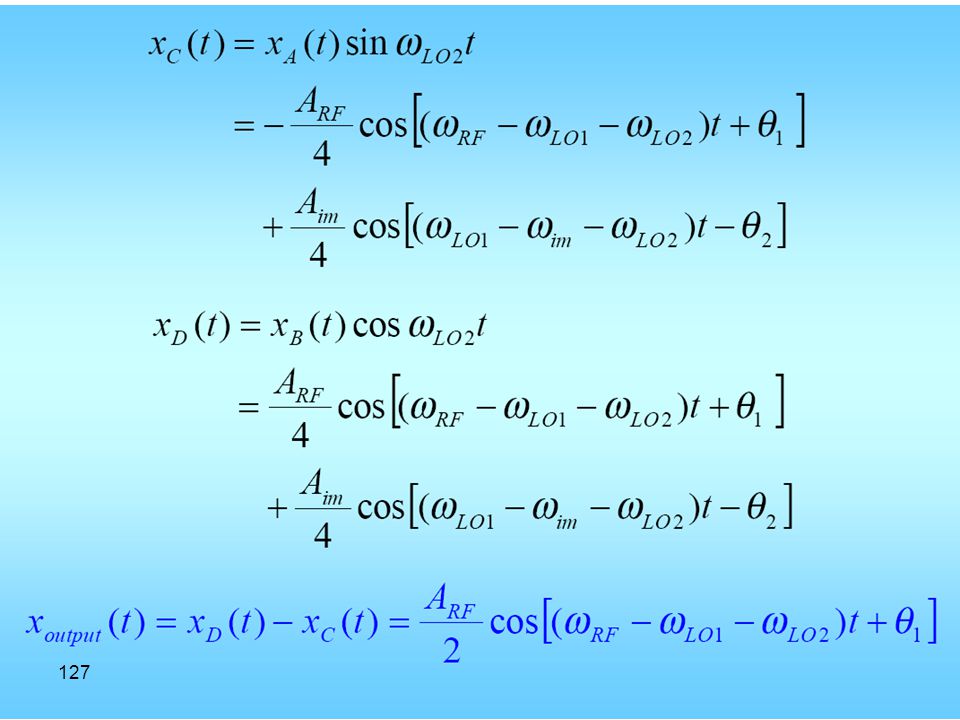
Weaver

128
RF Systems and Circuits
Spring 2014 RF Systems and Circuits

129
IRR

130
Input image power ratio

131
Gain Mismatch due to R, C errors
Spring 2014 RF Systems and Circuits Gain Mismatch due to R, C errors At w = 1/RC:

132
Weaver or Hartley? Hilbert transform is obtained using
Spring 2014 RF Systems and Circuits Weaver or Hartley? Hilbert transform is obtained using another quadrature (complex) mixing stage Advantages compared to Hartley: Better accuracy in generating the additional 90o phase shift IRR is limited to 40 dB, which is higher than Hartley architecture Disadvantages: Secondary image problem B. Razavi: RF Microelectronics, 2nd Edition
 mixing stage. Advantages compared to Hartley: Better accuracy in generating the additional 90o phase shift. IRR is limited to 40 dB, which is higher than Hartley architecture. Disadvantages: Secondary image problem. B. Razavi: RF Microelectronics, 2nd Edition.")
133
Direct Conversion Receiver
Spring 2014 RF Systems and Circuits Direct Conversion Receiver A single step down conversion is used. The output frequency is at DC B. Razavi: RF Microelectronics, 2nd Edition Advantages Disadvantages No image problem LO leakage Less complex / low power consumption DC offset Channel selection is done with a LPF Even order distortion Effect of mixer spurs are reduced Flicker noise IQ mismatch

134
Spring 2014 RF Systems and Circuits LO Leakage The LO signal can be leaked to the antenna by the capacitive coupling or substrate For singled ended Los, the LO leakage can reach -60 dBm Differential LO architectures have lower LO leakage (better than dBm) B. Razavi: RF Microelectronics, 2nd Edition
 B. Razavi: RF Microelectronics, 2nd Edition.")
135
Direct Conversion Receiver
Spring 2014 RF Systems and Circuits Direct Conversion Receiver DC Offset: The leaked LO signal can go through the antenna, LNA and down converted Because of the LO signal and its feedthrough signal carry the same frequency, a DC offset is produced (this phenomena is called LO self mixing). BB blocks usually have high again, hence the LO self mixing may saturate the receiver HPF are not common because they require a very low cut-off frequency (large components, slow settling) B. Razavi: RF Microelectronics, 2nd Edition
. BB blocks usually have high again, hence the LO self mixing may saturate. the receiver. HPF are not common because they require a very low cut-off frequency (large components, slow settling) B. Razavi: RF Microelectronics, 2nd Edition.")
136
Even Order Distortion RF Systems and Circuits
Spring 2014 RF Systems and Circuits Even Order Distortion B. Razavi: RF Microelectronics, 2nd Edition

137
Direct Conversion Receiver
Spring 2014 RF Systems and Circuits Direct Conversion Receiver Flicker Noise: For g the channel bandwidth is 10MHz. With a noise corner frequency of 200kHz For GSM, the channel bandwidth is 100 kHz and therefore a large portion of noise appears due to flicker noise B. Razavi: RF Microelectronics, 2nd Edition

138
Direct Conversion Receiver
Spring 2014 RF Systems and Circuits Direct Conversion Receiver IQ mismatch: mismatch in I and Q path affects SNR of received signals Mismatch effects are more dominate at high frequencies. Reducing the frequency at which the I and Q signal are generated enhances the SNR Digital calibration is used to correct these mismatches Amplitude mismatch: Phase mismatch:

139
Low-IF Receiver Has all the advantages of direct conversion receivers
Spring 2014 RF Systems and Circuits Low-IF Receiver Has all the advantages of direct conversion receivers More difficult image rejection requirements Minimum IF frequency is channel bandwidth DC offset is outside the signal bandwidth Complex Filter Large Requires matching Power hungry

140
Low IF receiver - Quadrature RF down conversion required
Spring 2014 RF Systems and Circuits Low IF receiver + Eliminate IF SAW, IF PLL and image filtering + Integration + Relaxes image rejection requirements + Avoids DC problems, relaxes 1/f noise problem - Quadrature RF down conversion required - Require higher performance ADC Additional mixer Slower RF PLL settling Even order distortion still problem Low freq IF filters require large chip area

141
Low-IF Down Conversion
Spring 2014 RF Systems and Circuits Low-IF Down Conversion Complex BPF Mirror signal, needs removal

142
Mirror Signal Suppression
Spring 2014 RF Systems and Circuits Mirror Signal Suppression Complex Bandpass Filter I Q I Q LO1 LO2

143
Complex Mixing- Real LO
Spring 2014 RF Systems and Circuits Complex Mixing- Real LO

144
Complex Mixing-Complex LO
Spring 2014 RF Systems and Circuits Complex Mixing-Complex LO

145
Spring 2014 RF Systems and Circuits Complex Mixing

146
Spring 2014 RF Systems and Circuits Bluetooth Receiver Has all the advantages of direct conversion receivers More difficult image rejection requirements Minimum IF frequency is channel bandwidth DC offset is outside the signal bandwidth

147
Direct Conversion Receiver
Spring 2014 RF Systems and Circuits Direct Conversion Receiver In Hartley architecture, it translates the RF signal to IF signal by the different phase of the local oscillator, sinwt and coswt. Finally, the i-phase and the q-phase signal with 90 degree phase shifter are combined at the output. Thus the image signal has been suppressed. Little image problem No IQ IF

148
Direct Conversion Receiver
Spring 2014 RF Systems and Circuits Direct Conversion Receiver LO is at same frequency as RF 1/f noise here can end up in channel Self mixing cause DC problem - Quadrature RF down conversion required - DC problem - Typically requires offset or 2x LO to avoid coupling + Eliminate IF SAW, IF PLL and image filtering + Integration + easier image problem

149
DC Offset (Self-mixing)
Spring 2014 RF Systems and Circuits DC Offset (Self-mixing) A D w c aLO(t)=ALOcos(w c+q) capacitive coupling substrate coupling bondwire coupling Saturates the following stages A D w c
 A. D. w c. aLO(t)=ALOcos(w c+q) capacitive coupling. substrate coupling. bondwire coupling. Saturates the following stages. A. D. w c.")
150
DC Offset (Self-mixing)
Spring 2014 RF Systems and Circuits DC Offset (Self-mixing) level DC Offset + - t
 level. DC Offset. + - t.")
151
DC Offset Cancellation
Spring 2014 RF Systems and Circuits DC Offset Cancellation Capacitive Coupling Requires a large capacitor Negative Feedback Nonlinear -A

152
Spring 2014 RF Systems and Circuits 1/f noise effect CMOS transistors has significant 1/f noise at low to DC frequency Significantly noise performance of direct conversion receivers Receive signal 1/f noise f

153
Even-Order Distortion
Spring 2014 RF Systems and Circuits Even-Order Distortion Interferers Dw y(t) = a1 x(t) + a2 x2(t) a2 A1A2 cos(Dw) Direct feed through Dw Direct feed through
 = a1 x(t) + a2 x2(t) a2 A1A2 cos(Dw) Direct feed through. Dw. Direct feed through.")
154
Mirror Signal Upper sideband and lower sideband are identical
Spring 2014 RF Systems and Circuits Mirror Signal Upper sideband and lower sideband are identical

155
Mirror Signal Upper sideband and lower sideband are not identical
Spring 2014 RF Systems and Circuits Mirror Signal Upper sideband and lower sideband are not identical

156
Mirror Signal Suppression
Spring 2014 RF Systems and Circuits Mirror Signal Suppression Quadrature Down Conversion A D 90 a(t) ui(t) uq(t) vi(t) vq(t) I Q
 ui(t) uq(t) vi(t) vq(t) I. Q.")
157
Quadrature Conversion
Spring 2014 RF Systems and Circuits Quadrature Conversion

158
Quadrature Down Conversion
Spring 2014 RF Systems and Circuits Quadrature Down Conversion

159
I/Q Mismatch RF Systems and Circuits I Phase & Gain Error a(t) Q 90
Spring 2014 RF Systems and Circuits I/Q Mismatch 90 I Q Phase & Gain Error a(t)
")
160
I/Q Mismatch due to LO errors
Spring 2014 RF Systems and Circuits I/Q Mismatch due to LO errors

161
RF Systems and Circuits
Spring 2014 RF Systems and Circuits

162
RF Systems and Circuits
Spring 2014 RF Systems and Circuits Use of I/Q down conversion recovers the nonsymmetrical receive signal spectrum But port isolation becomes more challenging Selfmixing and even order distortion may affect both channels and affect each other, causing additional I/Q mismatch

163
RF Systems and Circuits
Spring 2014 RF Systems and Circuits 90 a(t) A/D Base Band DSP Phase and gain mismatch compensation DC and 1/f cancellation
 A/D. Base. Band. DSP. Phase and gain mismatch. compensation. DC and 1/f. cancellation.")
164
Summary of Direct Conversion Receiver
Spring 2014 RF Systems and Circuits Summary of Direct Conversion Receiver No need for imager reject filter Suitable for monolithic integration with baseband DC offsets due to crosstalk of input ports of mixer Even order IM direct feed through to baseband Quadrature down conversion suppresses mirror I/Q mismatch due to mismatches in parasitics Low power consumption attributes to less hardware

165
Outline Friis Formula Merits of LNAs Common Gate LNA Common Source LNA
Spring 2014 RF Systems and Circuits Outline Friis Formula Merits of LNAs Common Gate LNA Common Source LNA Highly Linear LNA Wideband LNAs Mixers

166
Spring 2014 RF Systems and Circuits Cascaded Noise Figure In a line-up of receiver stages, use Friis equation Gi is the power gain Says that the noise factor ‘F’ is more influenced by earlier stages

167
LNA Merits Gain Low Noise (NF) High Linearity (IIP3)
Spring 2014 RF Systems and Circuits LNA Merits Gain Low Noise (NF) High Linearity (IIP3) Low Reflection (S11) High reverse isolation (S12) High Stability (K)
 High Linearity (IIP3) Low Reflection (S11) High reverse isolation (S12) High Stability (K)")
168
Common Gate LNA Input impedance is resistive (except for parasitics)
Spring 2014 RF Systems and Circuits Common Gate LNA Input impedance is resistive (except for parasitics) Offers good impedance match even at low frequencies
 Offers good impedance match even at low frequencies.")
169
Spring 2014 RF Systems and Circuits Common Gate LNA tunes out transistor and board parasitics. Channel resistance offers good reverse isolation

170
Common Gate LNA At matching condition, Zin = 1/gm
Spring 2014 RF Systems and Circuits Common Gate LNA At matching condition, Zin = 1/gm

171
Common Gate LNA: Lowering Power II
Spring 2014 RF Systems and Circuits Common Gate LNA: Lowering Power II Narrowband impedance transformer (L Section) allows the LNA to have Zin>50W. Transformer amplifies input signal by:
 allows the LNA to have Zin>50W. Transformer amplifies input signal by:")
172
Common Gate LNA: Lowering Power II
Spring 2014 RF Systems and Circuits Common Gate LNA: Lowering Power II For same IIP3, Veff has to increase by Current is reduced by the same factor Bias current is given by:

173
Common Source Amplifier
Spring 2014 RF Systems and Circuits Common Source Amplifier Input impedance is purely capacitive Resistive part appears at high frequency No input matching is possible

174
Common Source Amplifier
Spring 2014 RF Systems and Circuits Common Source Amplifier Rg is set to 50W => Input Matching Miller Effect due to Cgd => Limited Bandwidth

175
Common Source Amplifier
Spring 2014 RF Systems and Circuits Common Source Amplifier Cascode reduces Miller Effect Resistive Load limits linearity

176
Common Source Amplifier
Spring 2014 RF Systems and Circuits Common Source Amplifier Parallel Resonance at output boasts narrow band gain without impacting linearity Rg produces a lot of Noise NF>3 dB

177
Common Source Amplifier
Spring 2014 RF Systems and Circuits Common Source Amplifier Series resonance at input creates a resistive term Iin= jw CgsVgs Vin=Vgs+jwLs(Iin+gmVgs) gmVgs Iin
 gmVgs. Iin.")
178
Common Source Amplifier
Spring 2014 RF Systems and Circuits Common Source Amplifier Series resonance at input creates a resistive term @ RF, input is still capacitive because Ls is very small to give 50W with high wT

179
Common Source Amplifier
Spring 2014 RF Systems and Circuits Common Source Amplifier Gate inductance offers one more degree of freedom to allow matching and series resonance at the same time Valid for

180
Spring 2014 RF Systems and Circuits Parasitics Ali Niknejad ECE142

181
Design Procedure for Common Source LNAs
Spring 2014 RF Systems and Circuits Design Procedure for Common Source LNAs

182
Common Source Amplifier
Spring 2014 RF Systems and Circuits Common Source Amplifier Assume an equivalent resistive load Rd @ resonance

183
Common Source Amplifier
Spring 2014 RF Systems and Circuits Common Source Amplifier Noise Figure (F) is given by Source Coils Transistor Use samll Ls Decreases with wT
 is given by. Source. Coils. Transistor. Use samll Ls. Decreases with wT.")
184
Optimization of CS LNA Assume @ Input matching condition
Spring 2014 RF Systems and Circuits Optimization of CS LNA Assume @ Input matching condition

185
Optimization of CS LNA wT Increases Lg Noise dominates Higher power
Spring 2014 RF Systems and Circuits Optimization of CS LNA wT Increases Lg Noise dominates Higher power

186
Another Way to Look at It
Spring 2014 RF Systems and Circuits Another Way to Look at It If Q is input quality factor

187
Another Way to Look at It
Spring 2014 RF Systems and Circuits Another Way to Look at It The input is amplified by Q before it reaches the transistor This reduces linearity

188
Other Losses: Inductor Losses
Spring 2014 RF Systems and Circuits Other Losses: Inductor Losses Typically Lg losses dominate Adds in series to source noise Independent of FET gain

189
Other Losses: Gate Resistance
Spring 2014 RF Systems and Circuits Other Losses: Gate Resistance Gate Resistance creates additional noise (uncorrelated with channel noise) Use inter-digitated layout to reduce gate electrode resistance
 Use inter-digitated layout to reduce gate electrode resistance.")
190
Other Losses: Gate Induced Noise
Spring 2014 RF Systems and Circuits Other Losses: Gate Induced Noise Due to inversion layer resistance Partly correlated with conventional thermal noise Modeled as a resistance in series with gate

191
Other Losses: Gate Induced Noise
Spring 2014 RF Systems and Circuits Other Losses: Gate Induced Noise The effective Q is lowered by losses Higher Q is achieved through lower Cgs Smaller Cgs raises rinv and also gate resistance There is an optimum W at each current

192
Other Losses: Substrate Coupling
Spring 2014 RF Systems and Circuits Other Losses: Substrate Coupling BSIM3V3 models do NOT capture Cgb Gate to bulk capacitance is an additional path for noise

193
Other Losses: Substrate Coupling
Spring 2014 RF Systems and Circuits Other Losses: Substrate Coupling Hole distribution in the depletion layer are modulated by gate voltage Same effect on electrons in the inversion layer which reflects back on depletion region

194
Wideband CS LNA Uses an LC ladder filter to widen BW
Spring 2014 RF Systems and Circuits Wideband CS LNA Uses an LC ladder filter to widen BW Uses a large number of inductors Excellent noise performance

195
Resistive Feedback Feedback widens BW and lowers Zin
Spring 2014 RF Systems and Circuits Resistive Feedback Feedback widens BW and lowers Zin Power consumption is very high Noise Cancellation can be employed

196
Capacitive Cross Coupling Technique
Spring 2014 RF Systems and Circuits Capacitive Cross Coupling Technique Differential input impedance: Two voltage noise sources: vns & vn1 in each half circuit

197
Capacitive Cross-Coupling Technique
Spring 2014 RF Systems and Circuits Capacitive Cross-Coupling Technique The output differential noise current square due to each noise source is given by: Then: Using the input power matching condition:

Similar presentations


 Geometry (29%)>")


>")
 Transmitters Karl Davies East Kent Radio Society EKRS 1.>")


 Transmitters>")
 ANGLE MODULATION>")

, pressure.>")
