Download presentation
Presentation is loading. Please wait.

1
Sequential Circuit: Design BIL- 223 Logic Circuit Design Ege University Department of Computer Engineering

2
Sequential Circuits Inputs Outputs Next State Current State output logic next state logic C D Q Q C D Q Q' y x A A B Clock

3
Design Example: Sequence Recognizer A sequential circuit that recognizes the occurrence the bit sequence 1101 (The sequence 1101 must be recognized each time it occurs in the input sequence.) Thus, the sequential machine must remember that the first two one's have occurred as it receives another symbol. Input: X(t) {0, 1} Output: Z(t) {0, 1} Time 0 1 2 3 4 5 6 7 8 9 10 11 12 13 14 15 16 X(t) 1 0 0 1 0 1 1 0 1 0 1 1 0 1 1 0 1 Z(t) 0 0 0 0 0 0 0 0 1 0 0 0 0 1 0 0 1 3 3
 {0, 1} Output: Z(t) {0, 1} Time X(t) Z(t)")
4
Obtain The State Diagram Time 0 1 2 3 4 5 6 7 8 9 10 11 12 13 14 15 16 X(t) 1 0 0 1 0 1 1 0 1 0 1 1 0 1 1 0 1 Z(t) 0 0 0 0 0 0 0 0 1 0 0 0 0 1 0 0 1 4 4 S0S0 S1S1 1/0 0/0 S2S2 1/0 S3S3 0/0 1/0 0/0 1/1 A Mealy Machine
 Z(t) S0S0 S1S1 1/0 0/0 S2S2 1/0 S3S3 0/0 1/0 0/0 1/1 A Mealy Machine")
5
Obtain State Table From the State Diagram, we can fill in the State Table. Assign binary codes for the states 5 5 00 1/0 0/0 1/0 0/0 1/0 0/0 1/1 011011 Present State InputX Next State OutputZ ABAB 000000 001010 010000 011100 100110 101100 110000 111011 Present State AB Next State x = 0 x = 1 Output x = 0 x = 1 0 0 100 0 1 000 1 1 000 1 0 0 101

6
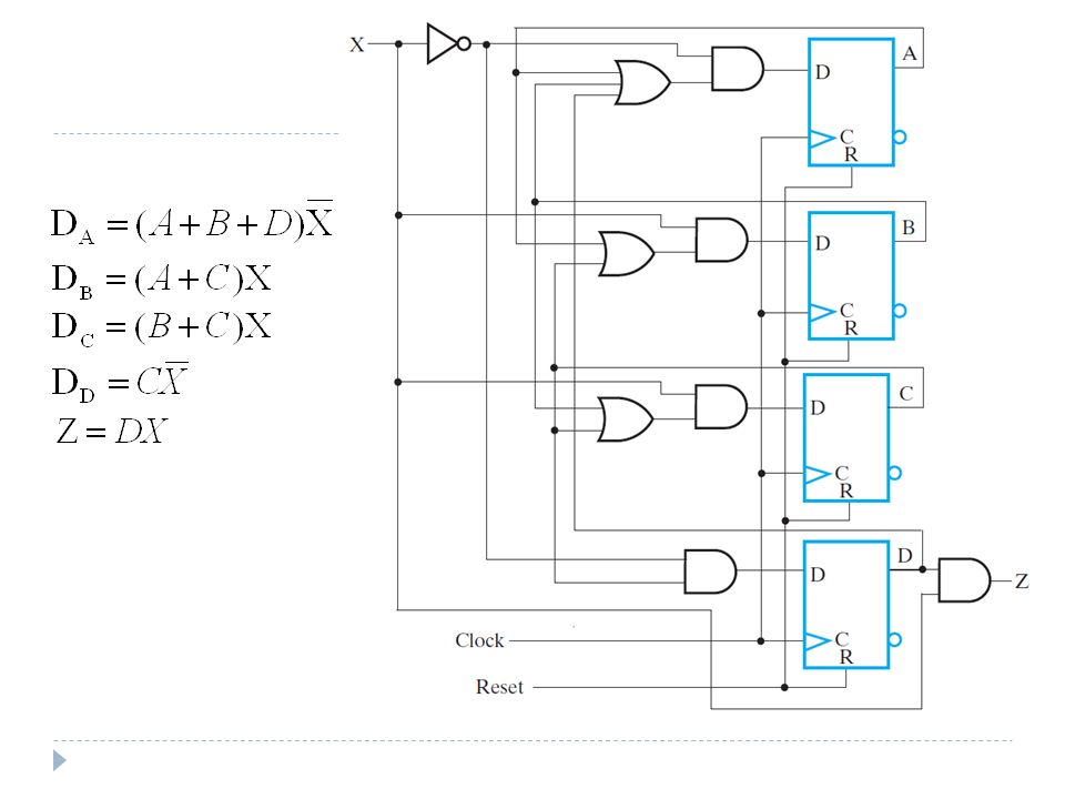
Find Flip-Flop Input and Output Equations Present State X Next State Z ABAB 000000 001010 010000 011100 100110 101100 110000 111011 00011110 0 0001 1 0101 X AB 00011110 0 0001 1 1010 X AB Select the flip-flop types. (D flip flop) Derive flip-flop input equations.
 Derive flip-flop input equations..")
7
Draw Logic Diagram Z X Clock

8
One Flip-flop per State (One-Hot) Assignment Provides simplified analysis and design Combinational logic may be simpler, but flip-flop cost higher 8 0001 1/0 0/0 1/0 0/0 1/0 0/0 1/1 0010 0100 1000 Present State Next State x = 0 x = 1 Output x = 0 x = 1 0001 001000 0001010000 1000010000 10000001001001
 Assignment Provides simplified analysis and design Combinational logic may be simpler, but flip-flop cost higher /0 0/0 1/0 0/0 1/0 0/0 1/ Present State Next State x = 0 x = 1 Output x = 0 x =")
10
Design Example: modulo 3 accumulator for 2- bit operands It adds each input operand to the stored sum, which is initially 0. Then takes the modulo. (2 + 0) modulo 3 = 2, (1+2) modulo 3 = 0 … Stored sum: (Y 1,Y 0 ), Input: (X 1,X 0 ), Output: (Z 1,Z 0 ) B/01 C/10 A/00 00 01 Reset Mealy or Moore?
 modulo 3 = 2, (1+2) modulo 3 = 0 … Stored sum: (Y 1,Y 0 ), Input: (X 1,X 0 ), Output: (Z 1,Z 0 ) B/01 C/10 A/ Reset Mealy or Moore .")
11
The State Machine Diagram Model (SMD) Y, Z S0 S1 Moore Outputs ABAB S2 A B A/Y, B/Z S0 S1 TCI Outputs ABAB S2 A B S0 S1 TCD Outputs A B/Y S2 (A B)/Z TCOD Outputs (A B) C/Y S0 S1 S2 ABAB C/Y Transition condition (TC) Transition condition-independent (TCI) Input Variables A, B, C Output Variables Y, Z Default: Y = 0, Z = 0 Transition condition-dependent (TCD) Transition and output condition-dependent (TCOD)
 Y, Z S0 S1 Moore Outputs ABAB S2 A B A/Y, B/Z S0 S1 TCI Outputs ABAB S2 A B S0 S1 TCD Outputs A B/Y S2 (A B)/Z TCOD Outputs (A B) C/Y S0 S1 S2 ABAB C/Y Transition condition (TC) Transition condition-independent (TCI) Input Variables A, B, C Output Variables Y, Z Default: Y = 0, Z = 0 Transition condition-dependent (TCD) Transition and output condition-dependent (TCOD)")
12
Example-1 What is the state table for this SMD? Y, Z A/Y BCBC S0 ABAB S2 A B S1 S3 A C ACAC B C/Y (B C)/Z A/Z BC Defaults: Y = 0, Z = 0 A/Y, B/Z
/Z A/Z BC Defaults: Y = 0, Z = 0 A/Y, B/Z.")
13
Example-2 What is the SMD for this state diagram?

Similar presentations

>")


 and Flow Tables UNIT 1 : Modeling Module 1.4 : Modeling Sequential circuits.>")


 =D A = AX + BX B(t+1) =D B = AX Y = AX + BX.>")


 and FSM Analysis (Lecture #17)>")
 and FSM Analysis (Lecture #19)>")
