Download presentation
Presentation is loading. Please wait.

1
Digital Electronics Lecture 6 Combinational Logic Circuit Design

2
Lecture 6 outline Review of last Lecture Design procedure for simple combinational logic circuits Continuation of Simulation exercises

3
Review of Last Lecture Simplification using K-map Simplification using logic converter in Multisim

4
DESIGN PROCEDURE FOR SIMPLE COMBINATIONAL LOGIC CIRCUIT 1- Write out the truth table for the required function. 2- From the truth table, write down the Boolean equation for the output. 3- Minimize the equation if appropriate. (using Karnough map). 4- Apply DeMorgan theorem as appropriate. 5- Draw out the circuit using NAND (or NOR) gates. Apply rules 4 and 5 if the circuit is restricted to one type of gates only.
. 4- Apply DeMorgan theorem as appropriate. 5- Draw out the circuit using NAND (or NOR) gates. Apply rules 4 and 5 if the circuit is restricted to one type of gates only..")
5
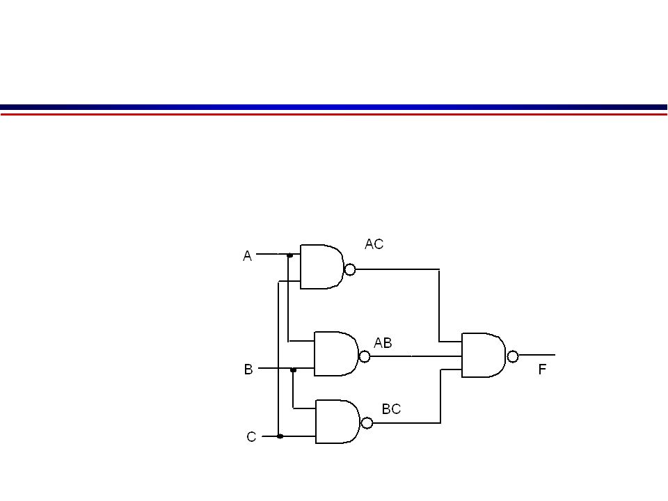
Example 1 Design a NAND gate Implementation of the following truth table. ABC F 0000 0010 0100Starting Point 0111 1000 1011 1101 1111

6
Using Boolean Algebra 2- F = A _ BC + AB _ C + ABC _ +ABC 3- Adding redundant term ABC many times. F = BC (A _ + A) + AC(B _ +B) + AB (C _ +C) F = BC + AC + AB 4- Apply DeMorgan theorem F = BC. AC. AB
 + AC(B _ +B) + AB (C _ +C) F = BC + AC + AB 4- Apply DeMorgan theorem F = BC. AC. AB.")
8
Example 2 This circuit is one of many employed in the arithmetic logic unit of a digital computer. It basically generates a Sum and a Carry simultaneously whilst adding a pair of one bit numbers. ABSumCarry 00 0 0 01 1 0 10 1 0 11 0 1 Sum = A _ B + AB _ Carry = A.B

9
FULL ADDER

10
Truth table ABCinSumCarry 00 00 0 00 1 1 0 01 01 0 01 10 1 10 0 1 0 10 10 1 11 00 1 11 11 1

11
S = A _ B _ C + A _ BC _ +AB _ C _ + ABC S = C (A _ B _ +AB) + C _ ( A _ B + AB _ ) S = C (A+B) + C _ ( A + B) S = A + B + C Co = A _ BC + AB _ C + ABC _ + ABC Co = C ( A _ B + AB _ ) + AB C = C(A + B) + AB
 + C _ ( A _ B + AB _ ) S = C (A+B) + C _ ( A + B) S = A + B + C Co = A _ BC + AB _ C + ABC _ + ABC Co = C ( A _ B + AB _ ) + AB C = C(A + B) + AB")
12
MULTIPLEXER A multiplexer (MUX) is a device that allows digital information from several sources to be routed onto a single line for transmission over the line to a common destination.
 is a device that allows digital information from several sources to be routed onto a single line for transmission over the line to a common destination.")
13
------------------------------------------------------------------- Data Select InputsInput Selected S1S0 -------------------------------------------------------- 00S _ 1 S _ 0 AA 01S _ 1 S0 BB 10S1 S _ 0 CC 11S1 S0 DD -------------------------------------------------------- X = S _ 1 S _ 0 A + S _ 1 S0 B + S1 S _ 0 C + S1 S0 D

14
Main Points Design procedure for combinational logic circuits. Adders Multiplexer Simulation exercises using logic converter

15
The End Thank you for your attention.

Similar presentations


 Digital Logic. Irvine, Kip R. Assembly Language for Intel-Based Computers, 2003. 2 NOT AND OR XOR NAND NOR Truth Tables Boolean.>")


 1 Feb Learning Objectives>")


