Download presentation
Presentation is loading. Please wait.

1
Lithography iTWG 2009 Summary
2009 Litho ITRS Update Lithography iTWG 2009 Summary

2
Outline Group Functions Table Groups – International
Various Techniques for Achieving Specifications Lithography Difficult Challenges Difficult Challenges > 22 nm Difficult Challenges < 22 nm (not 193) Lithography Technology Requirements Lithography Potential Solutions Table Groups – International Mask / Resist / EUVL / Imprint / Direct Write
 Lithography Technology Requirements. Lithography Potential Solutions. Table Groups – International. Mask / Resist / EUVL / Imprint / Direct Write.")
7
Future Fab Paper

9
2009 Litho Requirements Single Litho Tool Overlay

10
Table Sub Teams Litho – US, Japan, EU - Tables 1, 2, 3, EUVL Masks
– David Chan – Hayashi-san Optical Masks Table 5 Hayashi-san (DNP) Double Patterning - New – Harry Levinson Greg Hughes Resist Table 4 Team Ted Fedynshyn, Will Conley Imprint Masks – Doug Resnick and Lloyd Litt Other member- Hayashi-san Maskless – John Wiesner and Paul Petric
 Double Patterning - New. – Harry Levinson Greg Hughes. Resist Table 4 Team. Ted Fedynshyn, Will Conley. Imprint Masks. – Doug Resnick and Lloyd Litt. Other member- Hayashi-san. Maskless. – John Wiesner and Paul Petric.")
11
Optical Masks Table 5 Hayashi-san (DNP) Mr. Yasushi Ohkubo of HOYA
Mr. Yoji Tonooka of Toppan Mr. Iwao Higashikawa of Toshiba

12
Optical Mask - Excel

13
EUV Team Members

14
EUV Table Changes - Excel

16
E-mail Compromise between ITWG
Blank Defect Size Compromise between ITWG Japan – SELETE Data USA – Berkley Modeling C. Clifford IMEC – Rik Jonckheere

17
Comparison to Selete Data
This data matches very well. Selete is measuring the bump in one dark line. C. Clifford am measuring the space CD. The space CD change is two times larger than the bump in the dark line for a defect centered between the lines and normal incidence. Selete’s 5% and 10% lines can be compared to my 10% and 20% lines 17

18
[L2] Blank Defect Size —A blank defect is any unintended blank anomaly that prints or changes a printed image size by 10% or more. The mask defect size listed in the roadmap are the square root of the area of the smallest opaque or clear “defect” that is expected to print for the stated generation. This includes phase defects that may come from the substrate or multilayer. A phase defect is a defect that causes a phase change of around 180 deg. (For EUVL this would normally be a 3.5 nm height change.) It should be noted that smaller phase defects will also print but at a larger size limit. (ie a 90 deg defect will print at about 2X the size of the 180 deg defect)
![[L2] Blank Defect Size —A blank defect is any unintended blank anomaly that prints or changes a printed image size by 10% or more.](http://slideplayer.com/slide/696899/2/images/18/%5BL2%5D+Blank+Defect+Size+%E2%80%94A+blank+defect+is+any+unintended+blank+anomaly+that+prints+or+changes+a+printed+image+size+by+10%25+or+more..jpg "The mask defect size listed in the roadmap are the square root of the area of the smallest opaque or clear defect that is expected to print for the stated generation. This includes phase defects that may come from the substrate or multilayer. A phase defect is a defect that causes a phase change of around 180 deg. (For EUVL this would normally be a 3.5 nm height change.) It should be noted that smaller phase defects will also print but at a larger size limit. (ie a 90 deg defect will print at about 2X the size of the 180 deg defect).")
19
Double Patterning / Spacer Requirements
Double Patterning (LELE) Spacer Patterning Mask Requirments
 Spacer Patterning. Mask Requirments.")
20
Double Patterning & Spacer
Greg Hughes Harry Levinson (Global Foundries) Andrew J. Hazelton (Nikon) Christopher Bencher (Applied Materials) Mauro Vasconi (Numonyx)
 Andrew J. Hazelton (Nikon) Christopher Bencher (Applied Materials) Mauro Vasconi (Numonyx)")
23
Potential Solutions

24
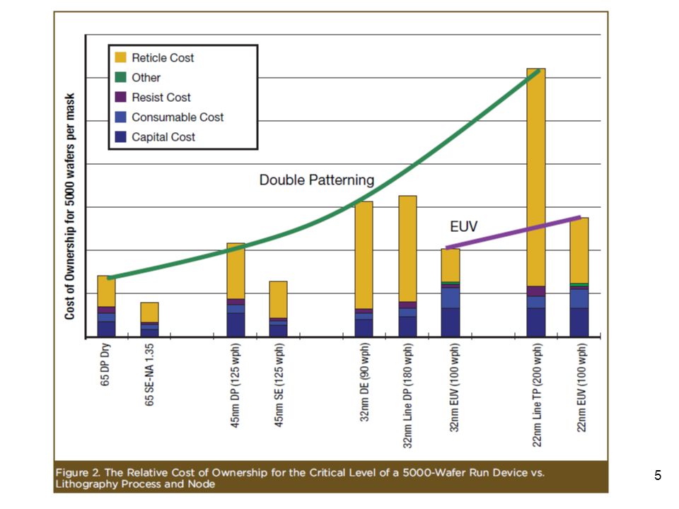
Summary Lithography solutions for 2010 Lithography solutions for 2013
45 nm half-pitch CoO is Driving 193 Immersion Single Exposure for DRAM/MPU Flash using Double Patterning (Spacer) for 32 nm half-pitch Lithography solutions for 2013 32 nm half-pitch Double patterning or EUV? for DRAM/MPU 22 nm half-pitch Double patterning or EUV for Flash Double exposure / patterning requires a complex set of parameters when different exposures are used to define single layers LER and CD Control Still remain as a Dominant Issue Mask Complexity for Double patterning Mask Infrastructure for EUV
 for 32 nm half-pitch. Lithography solutions for nm half-pitch Double patterning or EUV for DRAM/MPU. 22 nm half-pitch Double patterning or EUV for Flash. Double exposure / patterning requires a complex set of parameters when different exposures are used to define single layers. LER and CD Control Still remain as a Dominant Issue. Mask Complexity for Double patterning. Mask Infrastructure for EUV.")
Similar presentations