Download presentation
Presentation is loading. Please wait.

1
Chapter 6 Differential and Multistage Amplifiers The most widely used circuit building block in analog integrated circuits. Use BJTs, MOSFETS and MESFETs (metal semiconductor FET – read 5.12 – Gallium Arsenide-GaAs Device).
..")
2
Differential pair circuits are one of the most widely used circuit building blocks. The input stage of every op amp is a differential amplifier Basic Characteristics –Two matched transistors with emitters shorted together and connected to a current source –Devices must always be in active mode –Amplifies the difference between the two input voltages, but there is also a common mode amplification in the non- ideal case Let’s first understand how this circuit works.

3
Assume the inputs are shorted together to a common voltage, v CM, called the common mode voltage –equal currents flow through Q 1 and Q 2 –emitter voltages equal and at v CM -0.7 in order for the devices to be in active mode –collector currents are equal and so collector voltages are also equal for equal load resistors –difference between collector voltages = 0 What happens when we vary v CM ? –As long as devices in active mode, equal currents flow through Q 1 and Q 2 –Note: current through Q 1 and Q 2 always add up to I, current through the current source –So, collector voltages do not change and difference is still zero…. –Differential pair circuits thus reject common mode signals

4
Q 2 base grounded and Q 1 base at +1 V –All current flows through Q 1 –No current flows through Q 2 –Emitter voltage at 0.3V and Q 2 ’s EBJ not FB –v C1 = V CC - IR C –v C2 = V CC Q 2 base grounded and Q 1 base at -1 V –All current flows through Q 2 –No current flows through Q 1 –Emitter voltage at -0.7V and Q 1 ’s EBJ not FB –v C2 = V CC -aIR C –v C1 = V CC

5
Apply a small signal v i –Causes a small positive DI to flow in Q 1 –Requires small negative DI in Q 2 since I E1 +I E2 = I –Can be used as a linear amplifier for small signals (DI is a function of v i ) Differential pair responds to differences in the input voltage –Can entirely steer current from one side of the diff pair to the other with a relatively small voltage Let’s now take a quantitative look at the large- signal operation of the differential pair
 Differential pair responds to differences in the input voltage –Can entirely steer current from one side of the diff pair to the other with a relatively small voltage Let’s now take a quantitative look at the large- signal operation of the differential pair")
6
Large-Signal Operation First look at the emitter currents when the emitters are tied together Some manipulations can lead to the following equations and there is the constraint: Given the exponential relationship, small differences in v B1,2 can cause all of the current to flow through one side

7
Notice v B1 -v B2 ~= 4V T enough to switch all of current from one side to the other For small-signal analysis, we are interested in the region we can approximate to be linear –small-signal condition: v B1 -v B2 < V T /2

8
Small-Signal Operation Look at the small-signal operation: small differential signal v d is applied –expand the exponential and keep the first two terms multiply top and bottom by

9
Differential Voltage Gain For small differential input signals, v d << 2V T, the collector currents are… We can now find the differential gain to be…

10
Differential Half Circuit We can break apart the differential pair circuit into two half circuits – which then looks like two common emitter circuits driven by +v d /2 and – v d /2

11
We can then analyze the small-signal operation with the half circuit, but must remember –parameters r ,g m, and r o are biased at I/2 –input signal to the differential half circuit is v d /2 –voltage gain of the differential amplifier (output taken differentially) is equal to the voltage gain of the half circuit
 is equal to the voltage gain of the half circuit")
12
Common-Mode Gain When we drive the differential pair with a common-mode signal, v CM, the incremental resistance of the bias current effects circuit operation and results in some gain (assumed to be 0 when R was infinite)
")
13
If the output is taken differentially, the output is zero since both sides move together. However, if taken of the single circuit, the common-mode gain is finite If we look at the differential gain of the circuit, we get… Then, the common rejection ratio (CMRR) will be –which is often expressed in dB
 will be –which is often expressed in dB.")
14
CM and Differential Gain Equation Input signals to a differential pair usually consists of two components: common mode (v CM ) and differential(v d ) Thus, the differential output signal will be in general…
 and differential(v d ) Thus, the differential output signal will be in general…")
15
The BJT Differential Pair Use CD Implemented by a transistor circuit Connection to RC not essential to the operation Essential that Q1 and Q2 never enter saturation

16
Different Modes of Operation Differential pair with a common-mode input Common voltage I/2 vE = vCM-VBE vC1 = VCC – ( ½) I RC vC2 = VCC – ( ½) I RC vC1 – vC2 = ? Vary vCM (what happens?) Rejects common-mode
 Rejects common-mode.")
17
Differential pair with a large differential input Different Modes of Operation vB1 = +1 Q1 Q2 vE = 0.3 Keeps Q2 off vC1 = VCC - I RC vC2 = VCC

18
Differential pair with a large differential input o opposite polarity To that of (b) Different Modes of Operation
 Different Modes of Operation")
19
Differential pair with a small differential input Different Modes of Operation

20
Exercise 6.1

21
Large-Signal Operation of the BJT Differential Pair Equations Which can be manipulated to yield I I The collector currents can be obtained by multiplying the emitter currents by Alfa, which is ver close to unity

22
Large-Signal Operation of the BJT Differential Pair Relatively small difference voltage vB1 – vB2 will cause the current I to flow almost entirely in one of the two transistors. 4.VT (~100mV) is sufficient to switch the current to one side of the pair.
 is sufficient to switch the current to one side of the pair..")
23
Small-Signal Operation The Collector Currents When vd is applied ~ Multiplying by Assuming vd<<2VT Interpretation: IC1 increases by ic and iC2 decreases by ic

24
An Alternative Viewpoint Assume I to be ideal – its incremental resistance will be infinite and vd appears across a total resistance 2.re. A simple technique for determining the signal currents in a differential amplifier excited by a differential voltage signal v d ; dc quantities are not shown.

25
If emitter resistors are included A differential amplifier with emitter resistances. Only signal quantities are shown (on color).
..")
26
Input Differential Resistance This is the resistance-reflection rule; the resistance seen between the two bases is equal to the total resistance in the emitter circuit multiplied by the beta+1

27
Input Differential Resistance

28
Differential Voltage Gain The voltage gain is equal to the ratio of the total resistance in the collector circuit (2RC) to the total resistance in the emitter circuit (2re+2RE) ~
 to the total resistance in the emitter circuit (2re+2RE) ~")
29
Equivalence of the differential amplifier (a) to the two common-emitter amplifiers in (b). This equivalence applies only for differential input signals. Either of the two common-emitter amplifiers in (b) can be used to evaluate the differential gain, input differential resistance, frequency response, and so on, of the differential amplifier. Equivalence of the Differential Amp. To a Common-Emitter Amp. Differential amplifier fed in a complementary manner (push-pull or balanced) Base of Q1 raised Based of Q2 lowered
 can be used to evaluate the differential gain, input differential resistance, frequency response, and so on, of the differential amplifier. Equivalence of the Differential Amp. To a Common-Emitter Amp. Differential amplifier fed in a complementary manner (push-pull or balanced) Base of Q1 raised Based of Q2 lowered.")
30
Equivalent Circuit Model of a Differential Half-Circuit

31
Common-Mode Gain Assuming symmetry If output is taken single-endedly Acm and the differential gain Ad We can define CMRR Common-mode half-circuits Assuming non-symmetry

32
Input Common-Mode Resistance vCM ro Ricm = Ricm 2. Ricm vCM Equivalent common-mode half-circuit Since the input common-mode resistance is usually very large, its value will be affected by the transistor resistances R0 and r

33
Example 6.1 – Class Discussion

34
Example 6.3

37
Other Non-Ideal Characteristics Input Offset Voltage Input Bias and Offset Currents

38
Exercise 6.4

39
Biasing In BJT Integrated Circuits Many resistors, transistors and capacitors makes impossible to use conventional biasing methods Biasing in IC is based on the use of constant-current sources The Diode-Connected Transistor Shorting the base and the collector of a BJT results in a two- terminal device having an I-v characteristic identical ot the iE-vBE of the BJT. Since the BJT is still in active mode (vCB=0 results in an active mode operation) the current I divides between base and collector according to the value of the BJT Beta. Thus, the BJT still operates as a transistor in the active mode. This is the reason the I-v characteristics of the resulting diode is identical to the iE-vBE relationship of the BJT i
 the current I divides between base and collector according to the value of the BJT Beta. Thus, the BJT still operates as a transistor in the active mode. This is the reason the I-v characteristics of the resulting diode is identical to the iE-vBE relationship of the BJT i.")
40
Exercise 6.5

41
The Current Mirror Io Finite Beta and Early Effect For what value of would current mirror have a gain error 1%, 0.1 % Imperfection due to base current diverted from reference current I REF

42
Exercise 6.6

43
A Simple Current Source VCC VBE Neglecting the effect of finite beta and Dependence of Io and Vo, the output current Io will be equal IREF IoIREF

44
Exercise 6.7

45
Current-Steering Circuits Generation of a number of cross currents. IC Circuits 2 power supplies IREF is generated in the branch of the diode-connected transistor Q1, resistor R, and the diode-connected transistor Q2.

46
Exercise 6.9

47
Comparison With MOS Circuits 1 - The MOS mirror does not suffer from the finite Beta 2 – Ability to operate close to the power supply is an important issue on IC design 3 - Current Transfer: BJTs ~ relative areas; MOS ~ W/L 4 - VA lower for MOS Improved Current-Source Circuits

48
The Wilson Current Mirror Output resistance equal A factor greater the then simple Current source Disadvantage: reduced output swing. Observe that the voltage at the collector at Q3 has to be greater than the negative supply voltage by (vBB1 = VCEsat-3), which is about a volt.
, which is about a volt..")
49
Exercise 6.10 ~

50
Widlar Current Source It differs from the basic current mirror in an important way: a resistor RE is included in the emitter lead of Q2. Neglecting the base current we can write:

51
Example 6.2

52
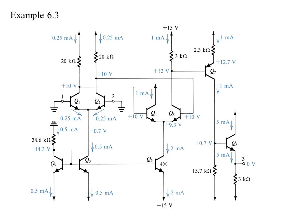
Example 6.3

54
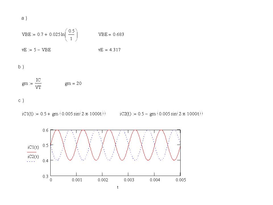
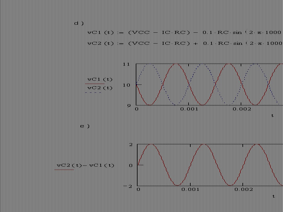
Current sources for biasing amplifying stages Multistage Amplifiers – Example 6.4 – pg. 552 Calculating 1 st stage gain -- Assuming Model Eqs. on Pg. 263 In the same manor k rR i 05.5)25101(2 )1(2 2 542 rrR i krrR id 2.20 21 k rrr e 1.10100*101 ))(1( 21 100 25. 21 E T I V ee rr )()( )( 1 E T C T m I V I V g r
25101(2 )1(2 2 542 rrR i krrR id k rrr e *101 ))(1( 21 E T I V ee rr )()( )( 1 E T C T m I V I V g r.")
55
Multistage Amplifiers – Example 6.4 – pg. 552 Calculating 1 st stage gain 1 Ri2 Total emitter resistance Total collector resistance

56
Multistage Amplifiers – Example 6.4 – pg. 552 Calculating 2 nd stage gain Ri3 re4 and re5 calc. before Potential gain is halved b/c converting to single-ended output

57
Multistage Amplifiers – Example 6.4 – pg. 552 Calculating 3 rd stage gain Purpose is to allow amplified signal to swing negatively Ri4

58
Multistage Amplifiers – Example 6.4 – pg. 552 Calculating 3 rd stage gain Overall Gain Output Resistance

59
The BJT Differential Amplifier With Active Load

60
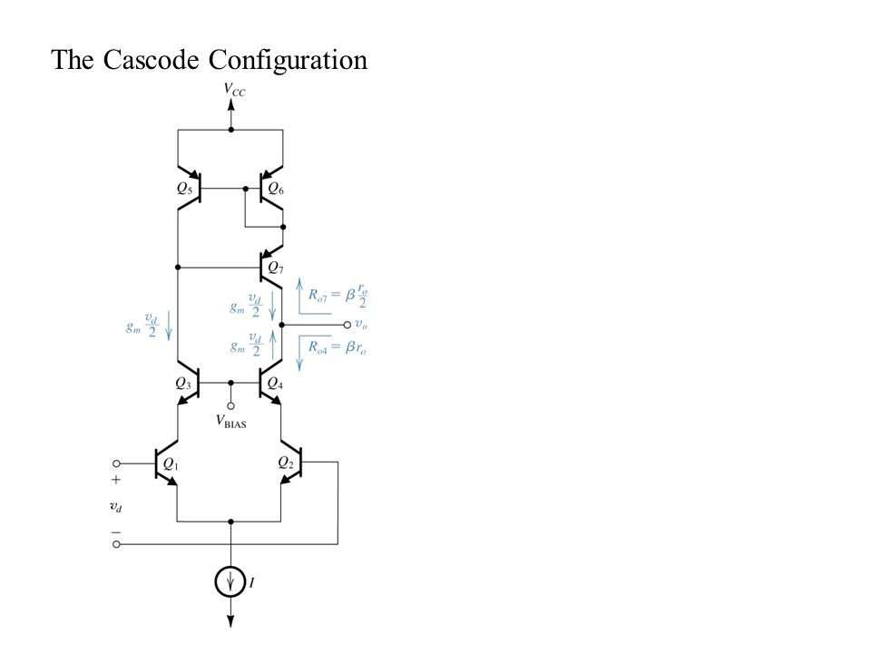
The Cascode Configuration

62
BJT Single Stage Common-Emitter Amplifier

63
MOSFET Operation

64
MOS Differential Amplifiers – MOS Differential Pair

65
MOS Differential Amplifiers – Offset Voltage

66
MOS Differential Amplifiers – Current Mirrors

67
Problem 6.1

68
Problem 6.15

69
BJT Differential Amplifier Laboratory Purpose The purpose of this lab is to investigate the behavior of a BJT difference amplifier. The circuit’s behavior needs to be modeled with theoretical equations and a computer simulation. Comparison of laboratory results with theoretical and simulated results is required for the relative validity of the models. This lab also investigates the variation of differential and common mode gains using a Monte Carlo analysis. Procedure Construct the circuit in Figure 1 on PSpice and a Jameco JE26 Breadboard using a Hewlett-Packard 6205 Dual DC Power Supply as the voltage sources and an MPQ2222 Bipolar Junction Transistor (Q2N2222). Using a Keithley 169 Digital Multi-Meter measure the voltages across the resistors to determine the transistor base current and collector current. From these current values calculate . Figure 1) Circuit for testing transistor value
. Using a Keithley 169 Digital Multi-Meter measure the voltages across the resistors to determine the transistor base current and collector current. From these current values calculate . Figure 1) Circuit for testing transistor value.")
70
Next construct the amplifier circuit shown in Figure 2. All transistors are MPQ2222 Bipolar Junction Transistors. Use PSpice to construct the circuit. Measure the DC values at the collector of Q1 and Q2. Do the measured values agree with theoretical ones. Measure the DC value at the emitter of Q1 and Q2. Do the measured value agree with the theoretical one. Indicate the inverting and non- inverting output. Input an AC signal into Q1 of your circuit at frequencies. What is the single voltage gain of your circuit? Figure 2

71
Both inputs (Vin1 and Vin2) should be then grounded in order to determine the DC operating point of the amplifier. Bias point voltages are measured and then compared to the bias points produced by the PSpice simulation. Record DC bias point data. Use a Wavetek 190 Function Generator with a sinusoidal input voltage of amplitude 0.031 V and apply to one of the input terminals and the other terminal remained grounded, as shown in figure 2. Use a Tektronix TDS 360 Digital Oscilloscope and a Fluke 1900A Multi-Meter the output of the amplifier to observe input signal frequencies. Determine the corner frequency (3-dB point) of the output and compared with the corner frequency generated with an AC sweep in PSpice. Plot the PSpice AC sweep simulation. Next calculate the differential mode voltage gain, A V-dm, from the laboratory data and compare to the A V-dm predicted by the PSpice simulation and theoretical equations. Both inputs are tied together to create a common mode signal on the input terminals. The output voltage is then used to calculate the common mode voltage gain, A V-cm, and then compared to the A V-cm predicted by the PSpice simulation and theoretical equations. From these values the common mode rejection ratio (CMRR) should be calculated for each case. Finally, PSpice should be used to perform a Monte Carlo analysis of the circuit. The resistors were all given standard unbridged values and were allowed to vary uniformly within 5% of the nominal resistor value. The transistors should be given a nominal value (say 175) and allowed to vary uniformly to +/- 100. The variations of differential and common mode gains should be graphed on two histograms.
 of the output and compared with the corner frequency generated with an AC sweep in PSpice. Plot the PSpice AC sweep simulation. Next calculate the differential mode voltage gain, A V-dm, from the laboratory data and compare to the A V-dm predicted by the PSpice simulation and theoretical equations. Both inputs are tied together to create a common mode signal on the input terminals. The output voltage is then used to calculate the common mode voltage gain, A V-cm, and then compared to the A V-cm predicted by the PSpice simulation and theoretical equations. From these values the common mode rejection ratio (CMRR) should be calculated for each case. Finally, PSpice should be used to perform a Monte Carlo analysis of the circuit. The resistors were all given standard unbridged values and were allowed to vary uniformly within 5% of the nominal resistor value. The transistors should be given a nominal value (say 175) and allowed to vary uniformly to +/ The variations of differential and common mode gains should be graphed on two histograms..")
72
Analysis / Questions What are the values of for the first transistor? (typical values of range from approximately 125 to 225) With the exception of the Monte Carlo analysis, all transistors were assumed to have this value in the PSpice simulations. All four transistors were contained within one integrated circuit so that hopefully there would be little change in values from one transistor to the next, making the previous assumption reasonably valid. How close are the measured DC bias points of the circuit to those predicted by the PSpice simulation? What is the reason for the small differences between measured and predicted voltages?
 With the exception of the Monte Carlo analysis, all transistors were assumed to have this value in the PSpice simulations. All four transistors were contained within one integrated circuit so that hopefully there would be little change in values from one transistor to the next, making the previous assumption reasonably valid. How close are the measured DC bias points of the circuit to those predicted by the PSpice simulation. What is the reason for the small differences between measured and predicted voltages .")
73
Exercises 6.17

74
An Active-Loaded CMOS Amplifier Exercise 6.19

75
BiCMOS Amplifiers Exercise 6.20

76
BiCMOS Amplifiers Exercise 6.21

77
BiCMOS Amplifiers Exercise 6.22

78
BiCMOS Current Mirrors and Differential Amplifiers

79
Gallium Arsenide (GaAs) Amplifiers Current sources – Exercise 6.23
 Amplifiers Current sources – Exercise 6.23")
80
Gallium Arsenide (GaAs) Amplifiers A Cascode Current Source – Exercise 6.24
 Amplifiers A Cascode Current Source – Exercise 6.24")
81
Gallium Arsenide (GaAs) Amplifiers Increasing The Output Resistance by Bootstrapping
 Amplifiers Increasing The Output Resistance by Bootstrapping")
82
Gallium Arsenide (GaAs) Amplifiers A Simple Cascode Configuration – The Composite Transistor
 Amplifiers A Simple Cascode Configuration – The Composite Transistor")
83
Gallium Arsenide (GaAs) Amplifiers Differential Amplifiers
 Amplifiers Differential Amplifiers")
84
Multistage Amplifiers Example 6.4

85
Multistage Amplifiers Example 6.5 SPICE Simulation of a Multistage Amplifier

Similar presentations


 Amplifiers>")


 The differential pair with a common-mode input signal vCM. (b) The differential.>")


