Download presentation
Presentation is loading. Please wait.

1
Interfacing of 8051 UNIT 4

2
Contents Interfacing of 7 segment display, LCD and keyboard.
Interfacing of DC motor, stepper motor and relay. Interfacing of ADC, DAC and sensors.

3
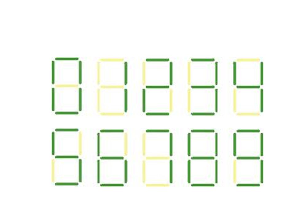
7 segment display

6
Interfacing of 7 segment display

7
7 segment code for CC DP G F E D C B A NUMBER 1 2 3

8
PROGRAM 7 SEGMENT DISPLAY
To display ‘1’ MOV A,#06H MOV P1,A SJMP $

9
LCD Interfacing

11
Pin No: Name Function 1 VSS This pin must be connected to the ground 2 VCC Positive supply voltage pin (5V DC) 3 VEE Contrast adjustment 4 RS Register selection 5 R/W Read or write 6 E Enable 7 DB0 Data 8 DB1 9 DB2 10 DB3 11 DB4 12 DB5 13 DB6 14 DB7 15 LED+ Back light LED+ 16 LED- Back light LED-

12
4 Decrement cursor (shift cursor to left)
1 Clear display screen 2 Return Home 4 Decrement cursor (shift cursor to left) 5 Increment cursor (shift cursor to right) 6 shift display right 7 shift display left 8 Display off, cursor off A Display off, cursor on C Display on, cursor off E Display on, cursor blinking F Display on, cursor blinking 10 Shift cursor position to left 14 Shift cursor position to right 18 Shift the entire display to the left 1C Shift the entire display to the right 80 Force cursor to the beginning of 1st line C0 Force cursor to the beginning of 2nd line 38 2 lines and 5 x 7 matrix
 5 Increment cursor (shift cursor to right) 6 shift display right. 7 shift display left. 8 Display off, cursor off. A Display off, cursor on. C Display on, cursor off. E Display on, cursor blinking. F Display on, cursor blinking. 10 Shift cursor position to left. 14 Shift cursor position to right. 18 Shift the entire display to the left. 1C Shift the entire display to the right. 80 Force cursor to the beginning of 1st line. C0 Force cursor to the beginning of 2nd line lines and 5 x 7 matrix.")
14
Interface Program MOV A,#38H // Use 2 lines and 5x7 matrix ACALL CMND MOV A,#0FH // LCD ON, cursor ON, cursor blinking ON ACALL CMND MOV A,#01H //Clear screen ACALL CMND MOV A,#06H //Increment cursor ACALL CMND MOV A,#82H //Cursor line one , position 2 ACALL CMND MOV A,#3CH //Activate second line ACALL CMND MOV A,#’W’ ACALL DISP MOV A,#’E’ ACALL DISP MOV A,#’L’ ACALL DISP MOV A,#’C’ ACALL DISP MOV A,#O ACALL DISP MOV A,#’M’ ACALL DISP MOV A,#’E’ ACALL DISP

15
CMND: MOV P1,A CLR P3.5 CLR P3.4 SETB P3.3 CLR P3.3 ACALL DELY RET;
DISP:MOV P1,A SETB P3.5 CLR P3.4 SETB P3.3 CLR P3.3 ACALL DELY RET;

16
DELY: MOV R0,#0FFH HERE: DJNZ R0, HERE RET; Subroutine CMND sets the logic of the RS, R/W, E pins of the LCD module so that the module recognizes the input data ( given to DB0 to DB7) as a command. Subroutine DISP sets the logic of the RS, R/W, E pins of the module so that the module recognizes the input data as a data to be displayed .
 as a command. Subroutine DISP sets the logic of the RS, R/W, E pins of the module so that the module recognizes the input data as a data to be displayed .")
17
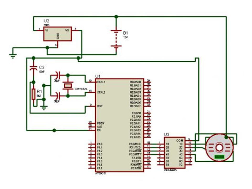
8051 & dc motor interface

19
ORG 00H // initial starting address MAIN: MOV P1,# B // motor runs clockwise ACALL DELAY // calls the 1S DELAY MOV P1,# B // motor runs anti clockwise ACALL DELAY // calls the 1S DELAY SJMP MAIN // jumps to label MAIN for repeating the cycle DELAY: MOV R4,#0FH WAIT1: MOV R3,#0FFH WAIT2: MOV R2,#0FFH WAIT3: DJNZ R2,WAIT3 DJNZ R3,WAIT2 DJNZ R4,WAIT1 RET END

20
Stepper Motor Interfacing
What is stepper motor? Stepper motors consist of a permanent magnetic rotating shaft, called the rotor, and electromagnets on the stationary portion that surrounds the motor, called the stator. a motor with a resolution of 5 degrees would move its rotor 5 degrees per step, thereby requiring 72 pulses (steps) to complete a full 360 degree rotation.
 to complete a full 360 degree rotation.")
21
Stepper motor operation

22
At position 1, we can see that the rotor is beginning at the upper electromagnet, which is currently active (has voltage applied to it). To move the rotor clockwise (CW), the upper electromagnet is deactivated and the right electromagnet is activated, causing the rotor to move 90 degrees CW, aligning itself with the active magnet. This process is repeated in the same manner at the south and west electromagnets until we once again reach the starting position.
, the upper electromagnet is deactivated and the right electromagnet is activated, causing the rotor to move 90 degrees CW, aligning itself with the active magnet. This process is repeated in the same manner at the south and west electromagnets until we once again reach the starting position.")
23
In the above example, we used a motor with a resolution of 90 degrees or demonstration purposes.
In reality, this would not be a very practical motor for most applications. The average stepper motor's resolution -- the amount of degrees rotated per pulse is much higher than this. You may double the resolution of some motors by a process known as "half-stepping".

25
Instead of switching the next electromagnet in the rotation on one at a time, with half stepping you turn on both electromagnets, causing an equal attraction between, thereby doubling the resolution. Both the top and right electromagnets are active, causing the rotor to position itself between the two active poles

29
Sequence Polarity Name Description Wave Drive, One-Phase Consumes the least power. Only one phase is energized at a time. Assures positional accuracy regardless of any winding imbalance in the motor. Hi-Torque, Two-Phase Hi Torque - This sequence energizes two adjacent phases, which offers an improved torque-speed product and greater holding torque.

30
---+ --++ --+- -++- -+-- ++-- +--- +--+
Half-Step Half Step - Effectively doubles the stepping resolution of the motor, but the torque is not uniform for each step. (Since we are effectively switching between Wave Drive and Hi-Torque with each step, torque alternates each step.) This sequence reduces motor resonance which can sometimes cause a motor to stall at a particular resonant frequency. Note that this sequence is 8 steps.
 This sequence reduces motor resonance which can sometimes cause a motor to stall at a particular resonant frequency. Note that this sequence is 8 steps.")
32
Stepper motor programming
org 0H stepper equ P3 main: mov stepper, #0CH acall delay mov stepper, #06H acall delay mov stepper, #03H acall delay mov stepper, #09H acall delay sjmp main delay: mov r7,#4 wait2: mov r6,#0FFH wait1: mov r5,#0FFH wait: djnz r5,wait djnz r6,wait1 djnz r7,wait2 ret

33
Analog to Digital Converter
Commonly used ADC device – ADC804 Pin out of ADC CS – Chip Select , active low RD – Read Digital data from ADC, H-L edge triggered WR -- Start conversion, L-H pulse edge triggered INTR -- end of conversion, Goes low to indicate conversion done Data bits -- D0-D7 CLK IN & CLK R – CLK IN is an input pin connected to an external clock source when an external clock is used for timing. However, ADC804 has an internal clock generator. To use the internal clock generator of the ADC804, the CLK IN and CLK R pins are connected to a capacitor and a resistor. In that case, the clock frequency is determined by the equation. f = 1/1.1RC R=10K and C=150pF f=606Hz the conversion time is 110us.

34
Input Voltage range of ADC
Vref/2 (Volts) Vin Step size (mV) Open (2.5) 0 to 5 5/256 = 19.53 2.56 0 to 5.12 5.12/256 =20 1.28 0 to 2.56 2.56/256 = 10 0.5 0 to 1 1/256=3.90
 Vin. Step size (mV) Open (2.5) 0 to 5. 5/256 = to /256 = to /256 = to 1. 1/256=3.90.")
35
Default 0-5V. Can be changed by setting different value for Vref/2 pin
Default 0-5V. Can be changed by setting different value for Vref/2 pin. Vin=Vin(+) – Vin (-) Range = 0 to 2x Vref/2. for Vin = 2x Vref/2. we get 256 as a digital output on D0-D7 Step Size a Smallest change – (2 x Vref/2)/ 256 for ADC804 for eg for step size 10mv ,digital output on D0-D7 changes by one count for every 10mv change of the input analog voltage.
 – Vin (-) Range = 0 to 2x Vref/2. for Vin = 2x Vref/2. we get 256 as a digital output on D0-D7. Step Size a Smallest change – (2 x Vref/2)/ 256 for ADC804. for eg for step size 10mv ,digital output on D0-D7 changes by one count for every 10mv change of the input analog voltage.")
36
Algorithm • Make CS=0 and send a low-to-high to pin WR to start the conversion. • Keep monitoring INTR – If INTR =0, the conversion is finished and we can go to the next step. – If INTR=1, keep polling until it goes low. • After INTR=0, we make CS=0 and send a high-to-low pulse to RD to get the data out of the ADC804 chip.

37
ADC Interfacing

38
ADC_IO: mov P1, #0xff ; To configure as input setb p3.4 clr p3.7 ;Chip select AGAIN setb P3.6 ;RD=1 clr P3.5 ;WR=0 setb P3.5 ;WR=1- low to high transition WAIT: jb P3.4, WAIT ;wait for INTR clr P3.6 ;RD=0 -High to low transition mov A, P1 ;read digital o/p sjmp AGAIN

39
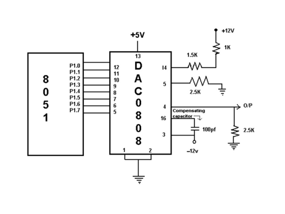
DAC Interfacing

42
Iout= Iref (D7/2+D6/4+D5/8+D4/16+D3/32+D2/64+D1/128+D0/256)
Vout=Iout x R

43
Interfacing of Relay with 8051

44
Interfacing LDR with 8051

Similar presentations


 addressable capability is unique to the 8051 Enables efficient handling.>")


.>")
