Download presentation
Presentation is loading. Please wait.

1
Diodes 1

2
Diode Class of non-linear circuits Uses
having non-linear v-i Characteristics Uses Generation of : DC voltage from the ac power supply Different wave (square wave, pulse) form generation Protection Circuits Digital logic & memory circuits
 form generation. Protection Circuits. Digital logic & memory circuits.")
3
Creating a Diode A diode allows current to flow in one direction but not the other. When you put N-type and P-type silicon together gives a diode its unique properties. A diode is the simplest possible semiconductor device. A diode allows current to flow in one direction but not the other. You may have seen turnstiles at a stadium or a subway station that let people go through in only one direction. A diode is a one-way turnstile for electrons. When you put N-type and P-type silicon together as shown in this diagram, you get a very interesting phenomenon that gives a diode its unique properties.

4
.

5
Diode Equivalent circuit in the reverse direction
Equivalent circuit in the forward direction.

6
Reverse Bias Forward Bias Operation -ve voltage is applied to Anode
Current through diode = 0 (cut off operation) Diode act as open circuit Forward Bias +ve voltage applied to Anode Current flows through diode voltage Drop is zero (Turned on) Diode is short circuit
 Diode act as open circuit. Forward Bias. +ve voltage applied to Anode. Current flows through diode. voltage Drop is zero (Turned on) Diode is short circuit.")
7
The two modes of operation of ideal diodes
sedr42021_0302a.jpg Reverse biased Reverse Voltage 10 V Forward biased Forward Current 10 mA

8
Ex 3.2

9
Rectifier circuit Equivalent circuit when vi 0 Waveform across diode
Input waveform Equivalent circuit when vi 0 sedr42021_0303a.jpg Output waveform. Equivalent circuit when vi ≤ 0 Waveform across diode

10
Exercise 3-3

13
Battery Charger sedr42021_0304a.jpg

14
Diode logic gates vy = vA.vB.vC vy = vA+vB+vC OR gate
AND gate (in a positive-logic system) sedr42021_0305a.jpg vy = vA.vB.vC vy = vA+vB+vC
 sedr42021_0305a.jpg. vy = vA.vB.vC. vy = vA+vB+vC.")
15
Diodes are ideal , Find the value of I and V
sedr42021_0306a.jpg Diodes are ideal , Find the value of I and V Figure 3.6 Circuits for Example 3.2.

16
Both Diodes are conducting
Example 3.2. sedr42021_0306a.jpg Assumption Both Diodes are conducting

17
Both Diodes are conducting
Assumption Both Diodes are conducting Node A Node B Not Possible Thus assumption of both diode conducting is wrong

18
Example 3.2(b). Assumption is correct Assumption # 2
Diodes 1 is not conducting Diodes 2 is conducting sedr42021_0306a.jpg Assumption is correct

19
Diodes are ideal , Find the value of I and V
sedr42021_e0304a.jpg Figure E3.4 Diodes are ideal , Find the value of I and V

20
Diodes are ideal , Find the value of I and V
Figure E3.4 Diodes are ideal , Find the value of I and V I= 2mA V= 0V I= 0A V= 5V I= 0A V= -5V I= 2mA V= 0V sedr42021_e0304a.jpg

21
Figure E3.4 Diodes are ideal , Find the value of I and V
sedr42021_e0304a.jpg I= 3mA V= 3V I= 4mA V= 1V

22
Diodes are ideal , Find the value of I and V
sedr42021_p03002a.jpg Diodes are ideal , Find the value of I and V Figure P3.2

23
Figure P3.2 Diodes are ideal , Find the value of I and V
Diode is conducting I = 0.6 mA V = -3V sedr42021_p03002a.jpg Diode is cut-off I = 0 mA V = 3V Diode is conducting I = 0.6 mA V = 3V Diode is cut-off I = 0 mA V = -3V

24
Problem 3-3 D1 Cut-Off & D2 Conducting I = 3mA
Diodes are ideal , Find the value of I and V sedr42021_p03003a.jpg D1 Cut-Off & D2 Conducting I = 3mA D1 Cut-Off & D2 Conducting I = 1mA , V=1 V

25
In ideal diodes circuits, v1 is a 1-kHz, 10V peak sine wave.
sedr42021_p03004a.jpg Figure P3.4 In ideal diodes circuits, v1 is a 1-kHz, 10V peak sine wave. Sketch the waveform of vo

26
In ideal diodes circuits, v1 is a 1-kHz, 10V peak sine wave.
Sketch the waveform of vo Vp+ = 10V Vp- = 0V f = 1 K-Hz Vp+ = 0V Vp- = - 10V f = 1 K-Hz Vo = 0V sedr42021_p03004a.jpg

27
Sketch the waveform of vo
Figure P3.4 In ideal diodes circuits, v1 s a 1-kHz, 10V peak sine wave. Sketch the waveform of vo Vp+ = 10V Vp- = -10V f = 1 K-Hz Vp+ = 10V Vp- = 0V f = 1 K-Hz Vp+ = 10V Vp- = 0V f = 1 K-Hz sedr42021_p03004a.jpg

28
Sketch the waveform of vo
Figure P3.4 In ideal diodes circuits, v1 s a 1-kHz, 10V peak sine wave. Sketch the waveform of vo sedr42021_p03004g.jpg

29
In ideal diodes circuits, v1 s a 1-kHz, 10V peak sine wave.
Figure P3.4 In ideal diodes circuits, v1 s a 1-kHz, 10V peak sine wave. Sketch the waveform of vo Vp+ = 0V Vp- = -10V f = 1 K-Hz V0 = 0V Vp+ = 10V Vp- = -5V f = 1 K-Hz sedr42021_p03004g.jpg

30
Sketch the waveform of vo
Figure P3.4 In ideal diodes circuits, v1 s a 1-kHz, 10V peak sine wave. Sketch the waveform of vo Vp+ = 10V Vp- = -5V f = 1 K-Hz sedr42021_p03004g.jpg

31
Problem 3-4(k) For Vi >0 V D1 is cutoff D2 is conducting vo=1V
For Vi < 0 V is conducting D2 is cutoff vo=vi+1V - 9 V

32
Problem 3-4(k)
")
33
Figure P3.6 sedr42021_p03006a.jpg X = A . B X = A + B

34
Problem 3-4 (c) vo=zero
 vo=zero")
35
Problem 3-4(f) +ve Half Cycle with 10 V peak at 1 KHz
Vi is a 1kHz 10-V peak sine wave. +ve Half Cycle with 10 V peak at 1 KHz

36
Problem 3-4(h) vo=zero
 vo=zero")
37
Problem 3.5 vi is 10 V peak sine wave and I = 100 mA current source. B is battery of 4.5 V . Sketch and label the iB 100 mA 4.5 v

38
Solution P3-5 100 mA vo 4.5 v

39
Problem 3-5 100 mA 4.5 v

40
Problem 3-5 10 4.5 100 mA

41
REVERSE POLARITY PROTECTOR

42
REVERSE POLARITY PROTECTOR
The diode in this circuit protects a radio or a recorder etc... In the event that the battery or power source is connected the wrong way round, the diode does not allow current to flow.

43
Problem 3-9 D1& D2 Conducting I1=1mA D1=off, D2=On I3=0.5 mA
sedr42021_p03009a.jpg D1& D2 Conducting I1=1mA I3=0.5 mA I2=0.5 mA V= 0 V D1=off, D2=On I1= I3=0.66 mA V = -1.7 V

44
Problem 3-10 D conducting I=0.225 mA I=0A V=4.5V V=-2V
sedr42021_p03010a.jpg D conducting I=0.225 mA V=4.5V D is not conducting I=0A V=-2V

45
Problem 3-16 V RED GREEN 3V On Off D1 conducts 0 V Off Off
-3 V Off On D2 conducts

46
Quiz No 3 DE 28 EE -A Sketch vO if vi is 8 sin
Find out the conduction angle for the diode & fraction of the cycle the diode is conducting

47
Solution Quiz No 3 8V I1 I2 vi/2 I

48
Vi<5V D2 is cut-off, Vo=5V Vi>5V D2 is conducts
Sketch vO if vi is 10 sin Find out the conduction angle for the diode & fraction of the cycle the diode is conducts D1 never conducts Vi<5V D2 is cut-off, Vo=5V Vi>5V D2 is conducts +12 V 5 D1 D2

49
Quiz No 3 DE 27 CE -B D1 never conducts Vi<5V D2 is cut-off, Vo=Vi
Sketch vO if vi is 10 sin Find out the conduction angle for the diode & fraction of the cycle the diode is conducts D1 never conducts Vi<5V D2 is cut-off, Vo=Vi Vi>5V D2 is conducts

50
Problem Assume the diodes are ideal, sketch vo if the input is 10sin (9) Find out the conduction angles for Diode D1 & D2 (4) and the fraction of the cycle these diodes conduct. (2)
 and the fraction of the cycle these diodes conduct. (2)")
52
-2V

53
Semiconductor materials
Germanium The earliest commercial semiconductor devices mostly used Germanium. This element has 32 electrons per atom and melts at 985 °C. It has now largely fallen into disuse because it is much rarer and more expensive than Silicon and has no real advantages for most purposes.

54
Current flow in Semiconductors
An electric current can flow through a semiconductor as a result of the movement of holes and/or free electrons. There are two important processes that account for current flow in semiconductors. These processes are called drift and diffusion.

55
Drift Applying an electric field across a semiconductor will cause holes and free electrons to drift through the crystal The total current is equal to the sum of hole current (to the right) and electron current (to the left).
 and electron current (to the left).")
56
Diffusion A drop of ink in a glass of water diffuses through the water until it is evenly distributed. The same process, called diffusion, occurs with semiconductors. If some extra free electrons are introduced into a p-type semiconductor, the free electrons will redistribute themselves so that the concentration is more uniform. The free electrons will tend to move to the right. This net motion of charge carriers constitutes a diffusion current. The free electrons move away from the region of highest concentration. The higher the localized concentration, the greater will be the rate at which electrons move away. The same process applies to holes in an n-type semiconductor. Note that when a few minority carriers are diffusing through a sample, they will encounter a large number of majority carriers. Some recombination will occur. A number of both types of carrier will be lost.

57
Two-dimensional representation of the silicon crystal.
sedr42021_0340.jpg The circles represent the inner core of silicon atoms, with +4 indicating its positive charge of +4q, which is neutralized by the charge of the four valence electrons. Observe how the covalent bonds are formed by sharing of the valence electrons. At 0 K, all bonds are intact and no free electrons are available for current conduction.

58
Two-dimensional representation of the silicon crystal.
sedr42021_0340.jpg 14 Electrons

59
Silicon Crystal All silicon atoms bond perfectly to four neighbors
Silicon Crystal All silicon atoms bond perfectly to four neighbors Leaving no free electrons to conduct electric current This makes a silicon crystal an insulator rather than a conductor.

60
Silicon Crystal Carbon, silicon and germanium -- each has four electrons in its outer orbital. The four valence electrons form perfect covalent bonds with four neighboring atoms, creating a lattice. In silicon, the crystalline form is a silvery, metallic-looking substance. All of the outer electrons in a silicon crystal are involved in perfect covalent bonds, so they can't move around. In spite of four valence electrons, a pure silicon crystal is nearly an insulator -- very little electricity will flow through it. Metals tend to be good conductors of electricity because they usually have "free electrons" that can move easily between atoms, and electricity involves the flow of electrons. While silicon crystals look metallic, they are not, in fact, metals. All of the outer electrons in a silicon crystal are involved in perfect covalent bonds, so they can't move around. A pure silicon crystal is nearly an insulator -- very little electricity will flow through it. Carbon, silicon and germanium (germanium, like silicon, is also a semiconductor) have a unique property in their electron structure -- each has four electrons in its outer orbital. This allows them to form nice crystals. The four electrons form perfect covalent bonds with four neighboring atoms, creating a lattice. In carbon, we know the crystalline form as diamond. In silicon, the crystalline form is a silvery, metallic-looking substance
 have a unique property in their electron structure -- each has four electrons in its outer orbital. This allows them to form nice crystals. The four electrons form perfect covalent bonds with four neighboring atoms, creating a lattice. In carbon, we know the crystalline form as diamond. In silicon, the crystalline form is a silvery, metallic-looking substance.")
61
Silicon and Germanium

62
Silicon Lattice

63
sedr42021_0341.jpg At room temperature, some of the covalent bonds are broken by thermal ionization. Each broken bond gives rise to a free electron and a hole, both of which become available for current conduction.

64
Intrinsic Semiconductor Electrons and holes

65
Semiconductor Current

66
The Valence Band The valence band is the band made up of the occupied molecular orbitals and is lower in energy than the so-called conduction band. It is generally completely full in semi-conductors. When heated, electrons from this band jump out of the band across the band gap and into the conduction band, making the material conductive.

67
The Fermi Level The Fermi Level is defined as the highest occupied molecular orbital in the valence band at 0 K, so that there are many states available to accept electrons, if the case were a metal. It should be noted that this is not the case in insulators and semiconductors since the valence and conduction bands are separated. Therefore the Fermi-Level is located in the band gap. The probability of the occupation of an energy level is based on the Fermi function

68
Conduction Band The conduction band is the band of orbitals that are high in energy and are generally empty. In reference to conductivity in semiconductors, it is the band that accepts the electrons from the valence band.

69
Doping Silicon You can change the behavior of silicon and turn it into a conductor by doping it. In doping, you mix a small amount of an impurity into the silicon crystal. There are two types of impurities: .N-type P-type -. A minute amount of either N-type or P-type doping turns a silicon crystal from a good insulator into a viable conductor -- hence the name "semiconductor." N-type and P-type silicon are not that amazing by themselves; but when you put them together, you get some very interesting behavior at the junction. You can change the behavior of silicon and turn it into a conductor by doping it. In doping, you mix a small amount of an impurity into the silicon crystal. There are two types of impurities: N-type - In N-type doping, phosphorus or arsenic is added to the silicon in small quantities. Phosphorus and arsenic each have five outer electrons, so they're out of place when they get into the silicon lattice. The fifth electron has nothing to bond to, so it's free to move around. It takes only a very small quantity of the impurity to create enough free electrons to allow an electric current to flow through the silicon. N-type silicon is a good conductor. Electrons have a negative charge, hence the name N-type. P-type - In P-type doping, boron or gallium is the dopant. Boron and gallium each have only three outer electrons. When mixed into the silicon lattice, they form "holes" in the lattice where a silicon electron has nothing to bond to. The absence of an electron creates the effect of a positive charge, hence the name P-type. Holes can conduct current. A hole happily accepts an electron from a neighbor, moving the hole over a space. P-type silicon is a good conductor. A minute amount of either N-type or P-type doping turns a silicon crystal from a good insulator into a viable (but not great) conductor -- hence the name "semiconductor." N-type and P-type silicon are not that amazing by themselves; but when you put them together, you get some very interesting behavior at the junction
 conductor -- hence the name semiconductor. N-type and P-type silicon are not that amazing by themselves; but when you put them together, you get some very interesting behavior at the junction.")
70
The Doping of Semiconductors
. The Doping of Semiconductors The addition of a small percentage of foreign atoms in the regular crystal lattice of silicon or germanium produces dramatic changes in their electrical properties, producing n-type and p-type semiconductors. Pentavalent impurities Impurity atomw with 5 valence electrons produce n-type semiconductors by contributing extra electrons. Trivalent impurities Impurity atoms with 3 valence electrons produce p-type semiconductors by producing a "hole" or electron deficiency.

71
Valence Electrons

72
N - Type Silicon Doping In N-type doping, phosphorus or arsenic is added to the silicon in small quantities. Phosphorus and arsenic each have five outer electrons, The fifth electron has nothing to bond to, So it's free to move around. It takes only a very small quantity of the impurity to create enough free electrons to allow an electric current to flow through the silicon. N-type silicon is a good conductor. Electrons have a negative charge, hence the name N-type

73
A silicon crystal doped by a pentavalent element.
sedr42021_0343.jpg A silicon crystal doped by a pentavalent element. Each dopant atom donates a free electron and is thus called a donor. The doped semiconductor becomes n type.

74
N Type sedr42021_0343.jpg

75
N-Type Semiconductor N-Type Semiconductor
The addition of pentavalent impurities such as antimony, arsenic or phosphorous contributes free electrons, greatly increasing the conductivity of the intrinsic semiconductor. Phosphorous may be added by diffusion of phosphine gas (PH3).
.")
76
P – Type Silicon Doping In P-type doping, boron or gallium is the dopant. Boron and gallium each have only three outer electrons. When mixed into the silicon lattice, they form "holes" in the lattice where a silicon electron has nothing to bond to. The absence of an electron creates the effect of a positive charge, hence the name P-type. Holes can conduct current. A hole happily accepts an electron from a neighbor, moving the hole over a space. P-type silicon is a good conductor.

77
A silicon crystal doped with a trivalent impurity.
sedr42021_0344.jpg A silicon crystal doped with a trivalent impurity. Each dopant atom gives rise to a hole The semiconductor becomes p type.

78
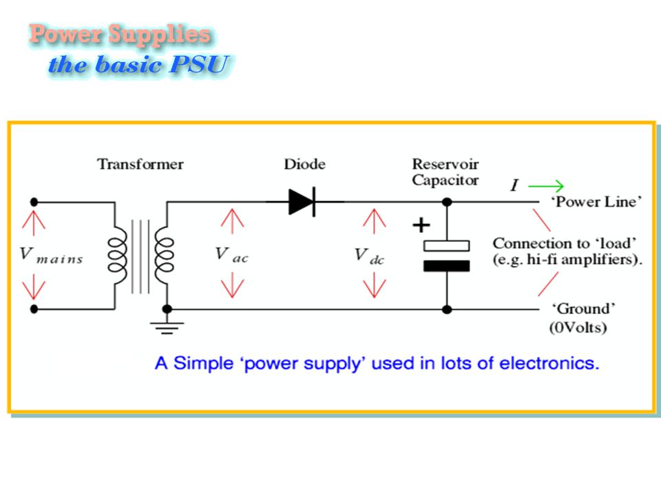
P Type sedr42021_0344.jpg

79
P-Type Semiconductor P-Type Semiconductor
P-Type Semiconductor The addition of trivalent impurities such as boron, aluminum or gallium to an intrinsic semiconductor creates deficiencies of valence electrons,called "holes". It is typical to use B2H6 diborane gas to diffuse boron into the silicon material.

80
n and p Type Semiconductors

81
Bands for Doped Semiconductors
The application of band theory to n-type and p-type semiconductors shows that extra levels have been added by the impurities. In n-type material there are electron energy levels near the top of the band gap so that they can be easily excited into the conduction band. In p-type material, extra holes in the band gap allow excitation of valence band electrons, leaving mobile holes in the valence band

82
P-N Junction

83
P-N Junction In practice, both the p and n region are part of the same silicon crystal pn junction is formed within a single silicon crystal by creating region of different doping (p & n regions) Atoms are held in the position by bonds – called convalent bond formed by its four reliance electrons. At low temperature, no free electrons are available
 Atoms are held in the position by bonds – called convalent bond formed by its four reliance electrons. At low temperature, no free electrons are available.")
84
At room temperature, some of the bonds are broken by thermal ionization & some electrons are freed.
Parent atom is left with positive charge after electron leaves. This attracts electrons form a neighboring atoms & other atoms is positively charge. Process repeats & Holes are available to conduct electric current Electrons fill the hole & this process is known as recombination.

85
Two Mechanisms Diffusion
Associated with random motion of electrons & holes due to thermal agitation with uniform concentration of free electrons & holes no net flow of charge is resulted (no current) if concentration of say free electrons (or holes) is higher in one part of silicon then the other (doping), electrons will diffuse from the region of higher concentration to the region of lower concentration
 if concentration of say free electrons (or holes) is higher in one part of silicon then the other (doping), electrons will diffuse from the region of higher concentration to the region of lower concentration.")
86
Two Mechanisms This diffusion process given rise to a net flow of charge & diffusion current Drift Carrier drift occurs when an electric field is applied across a piece of silicon Electronic & Holes are accelerated by the electric field & acquire a velocity component (superimposed on the velocity of then thermal motion) called Drift velocity Causing Drift current flow
 called Drift velocity. Causing Drift current flow.")
87
Doped Semiconductor Material in which one kind (Electrons & Holes) predominate – majority of charged carrier are electron for n type & majority of charged carrier are holes for p types Phosphorus impurity donated electrons (donor) Boron impurity donated holes (Acceptor)
 predominate – majority of charged carrier are electron for n type & majority of charged carrier are holes for p types. Phosphorus impurity donated electrons (donor) Boron impurity donated holes (Acceptor)")
88
p-n Junction P Junction N Junction Concentration of holes is high
Majority charge carrier are hole N Junction Concentration of electron is high Majority charge carrier are electron

89
Diffusion Current ID Hole diffuse across the junction from the p side to the n side & similarly electron Two current components add together to form the diffusion current with direction from p to n side

90
Depletion Region Recombination of Hole & electrons take close to the junction thus depletion region is formed on both side of the junction Region acts as a barrier that has to be overcome for holes to diffuse into the n region & same is true for electron thus causing Diffusion Current ID to flow from p side to n side

91
Drift Current Is Diffusion current due to majority carrier diffusion
A component due to minority carrier drift exists across the junction

92
p-n Junction Due to electric field applied across the p-n junction
Electrons are moved by drift from p to n junction Holes are moved by drift from n to p junction Add together to form the drift current Is Direction of Isis from n to p junction Drift current is carried by thermally generated minority p carriers Drift current value depends upon temperature Independent of the value of the depletion layer voltage vo Under operative circuit conditions no external current flows ID = IS

93
p-n Junction open circuit
Junction Built in Voltage Vo will depends upon Temperature Doping Concentration Depletion region width Same on both side of p & n junction if doping levels are equal If doping levels are not equal the depletion layer will extend deeper into the more lightly doped material

94
The pn junction with no applied voltage (open-circuited terminals).
sedr42021_0345a.jpg The pn junction with no applied voltage (open-circuited terminals). (b) The potential distribution along an axis perpendicular to the junction.
. (b) The potential distribution along an axis perpendicular to the junction.")
95
Depletion Region

96
Forward Biased Conduction

97
The polarity of applied voltage which can't produce any current is called Reverse Bias.
The polarity of applied voltage which causes charge to flow through the diode is called Forward Bias.

99
To avoid breakdown, I is kept smaller than IS.
The pn junction excited by a constant-current source I in the reverse direction. To avoid breakdown, I is kept smaller than IS. Note that the depletion layer widens and the barrier voltage increases by VR volts, which appears between the terminals as a reverse voltage. sedr42021_0346.jpg

100
sedr42021_0347.jpg The charge stored on either side of the depletion layer as a function of the reverse voltage VR.

101
The pn junction excited by a reverse-current source I, where I > IS.
The junction breaks down, and a voltage VZ , with the polarity indicated, develops across the junction. sedr42021_0348.jpg

102
The pn junction excited by a constant-current source supplying a current I in the forward direction.
The depletion layer narrows and the barrier voltage decreases by V volts, which appears as an external voltage in the forward direction. sedr42021_0349.jpg

103
Minority-carrier distribution in a forward-biased pn junction.
sedr42021_0350.jpg Minority-carrier distribution in a forward-biased pn junction. It is assumed that the p region is more heavily doped than the n region; NA @ ND.

104
Terminal Characteristics of a Junction Diode

105
The diode i–v relationship
sedr42021_0308.jpg The diode i–v relationship with some scales expanded and others compressed in order to reveal details.

106
Terminal Characteristics of a Junction Diode
Forward Biased Region v > 0 Reversed Biased Region v < 0 Breakdown Region v < -VZK

107
Forward Biased Region Is Saturation current – Scale Current
Is is constant at a given temperature Is is directly proportional to Cross-Sectional region of the diode, Is doubles if cross-sectional area is double Is is A for small size diode Doubles in value for every 10OC rise in temperature

108
Forward Biased Region Thermal Voltage VT
VT = kT/q K = Boltzmann’s constant = 1.38 X Joules/Kelvin T = Absolute Temperature in Kelvin (273 +Temp in Co) q = Magnitude of charge = 1.6 X Coulombs 20oC is 25.2mV, ~ 25 mV n is 1 or 2 depending on the material and the physical structure of the diode n = 1 for Germanium Diode & n=2 for Silicon
 q = Magnitude of charge = 1.6 X Coulombs. 20oC is 25.2mV, ~ 25 mV. n is 1 or 2 depending on the material and the physical structure of the diode. n = 1 for Germanium Diode & n=2 for Silicon.")
109
Switching of a Diode The switching speed of a diode depends upon:
its construction and fabrication. In general the smaller the chip the faster it switches, other things being equal. The chip geometry, doping levels, and the temperature at nativity determine switching speeds . The reverse recovery time, trr, is the time it takes a diode to switch from on to off.

110
i >> Is Forward Biased Region
b Relationship of the current i to the voltage v holds good over many decades of current (seven decades, a factor of 107

111
Forward Biased Region

112
Forward Biased Region for v drop changes by for n = 1 for n = 2

113
Illustrating the temperature dependence of the diode forward characteristic
sedr42021_0309.jpg At a constant current, the voltage drop decreases by approximately 2 mV for every 1C increase in temperature.

114
At 20o C Reverse current Is = 1V/1M Ω= 1μ A
Figure E3.9 If V=1V at 20o C, Find V at 400C and 00C Is sedr42021_e0309.jpg At 20o C Reverse current Is = 1V/1M Ω= 1μ A Since the reverse leakage current doubles for every 100 C increase, At 400 C I = 4*1 = 4 μ A V = 4 μ A * 1MΩ = 4.0 V At 0 C I = ¼ μ A V = 0.25 V

115
Forward biased Diode Characteristics Example 3.3
A silicon diode displays a forward voltage of 0.7 V at a current of 1mA. Find Is at n=1 & 2

116
Ex 3.7 Silicon Diode with n=1 has i=1mA. Find voltage drop at i=0.1mA & 10mA

117
Solution P3-18 (a) At what forward voltage does a diode for which n=2 conduct a current equal to 1000Is? (b) In term if Is what current flows in the same diode when its forward voltage is 0.7 V
 In term if Is what current flows in the same diode when its forward voltage is 0.7 V.")
118
Problem 3-23 The circuit shown utilizes three identical diodes having n=1 and Is= A. Find the value of the current I required to obtain an output voltage Vo=2 V. Assume n=1 If a current of 1mA is drawn away from the output terminal by a load, what if the change in the output voltage. Assume n=1

119
Solution 3-23 The circuit shown utilizes three identical diodes having n=1 and Is= A. Find the value of the current I required to obtain an output voltage Vo=2 V. If a current of 1mA is drawn away from the output terminal by a load, what if the change in the output voltage.

120
Problem 3-25 In the circuit shown, both diode have n=1, but D1 has 10 times the junction area of D2. What value of V results?

121
In the circuit shown, both diode have n=1, but D1 has 10 times the junction area of D2. What value of V results? Solution 3-25(a)
")
122
To obtain a value of 50 mV, what current I2 id needed.
solution 2-25 (b) To obtain a value of 50 mV, what current I2 id needed.
 To obtain a value of 50 mV, what current I2 id needed.")
123
Problem 3-26 For the circuit shown, both diodes are identical, conducting 10mA at 0.7 V and 100 mA at 0.8 V. Find ‘n’ Find the value of R for which V = 80 m V.

124
Solution 3-26 (a) Find η Find R if Vo=80mV
 Find η Find R if Vo=80mV")
125
sedr42021_p03028.jpg Figure P3.28

126
Problem 3.36 Assuming identical diodes for which VD ID=1mA. Find R if V0 = 3 V

127
Modeling the Diode Forward Characteristics

128
A simple circuit used to illustrate the analysis of circuits in which
the diode is forward conducting. sedr42021_0310.jpg

129
Graphical analysis of the circuit using the exponential diode model.
sedr42021_0311.jpg

130
Iterative Analysis using the Exponential Model
Determined the diode current ID and Diode voltage VD with VDD =5V and R =1000 ohms. Diode has a current of a VD of .7 V, and that its voltage drop changes by 0.1 V for every decade change in current.

131
Solution

132
The Piecewise-Linear Model

133
Approximating the diode forward characteristic with two straight lines: the piecewise-linear model.
sedr42021_0312.jpg

134
The Piecewise-Linear Model
Exponential curve is approx into two straight lines Line No 1 with zero slope & Line 2 with a slope of 1/rd The voltage change of less than 50 mV is observed in case the current change from 0.1 mA to 10 mA.

135
Piecewise-linear model of the diode forward characteristic and its equivalent circuit representation. sedr42021_0313a.jpg

136
Piecewise-linear model
sedr42021_0314.jpg

137
The Constant – Voltage Drop Model

138
Constant – Voltage Drop Model
Forward conducting diode exhibits a constant voltage drop VD The voltage change of less than 50 mV is observed in case the current change from 0.1 mA to 10 mA. Model is used when Detailed information about diode characteristics in not available

139
Constant-voltage-drop model
sedr42021_0315.jpg

140
The constant-voltage-drop model of the diode forward characteristics and its equivalent-circuit representation. sedr42021_0316a.jpg

141
Ex 3.12 Design a cct to provide an output of 2.4 V with available diodes have a current of a VD of 0.7 V, and that its voltage drop changes by 0.1 V for every decade change in current.

142
Solution Ex 3.12 Voltage drop changes by 0.1 V for every decade change in current

143
Solution

144
The Small – Signal Model
A small ac signal is superimposed on the DC components. First determined dc Operating Point Then small signal operation around the operating point Small portion of the curve is approximated as almost linear segment of the diode characteristics.

145
The Small – Signal Model

146
sedr42021_0317a.jpg Figure Development of the diode small-signal model. Note that the numerical values shown are for a diode with n = 2.

147
The Small – Signal Model

148
The Small – Signal Model

149
Modeling the Diode Forward Characteristic
sedr42021_tb0301.jpg

150
sedr42021_tb0307.jpg Table 3.1 (Continued)
")
153
Exp 3-6 + - VD ID vd

154
Solution Input variation of 10% resulted in output voltage
variation of mV(0.8%) Voltage regulation
 Voltage regulation.")
155
Exercise 3-16 Design a circuit shown so that Vo=3v when IL =0 A and Vo changes by 40 mV per 1mA of diode current. (a) Find the value of R (b) The junction area of each diode relative to a diode with ).7 V drop at 1mA current. Assume n=1
 Find the value of R. (b) The junction area of each diode relative to a diode with ).7 V drop at 1mA current. Assume n=1.")
156
Excercise 3-16 Why 4 diodes and not 5? Diodes will not conduct at 0.6 V

157
Diode Forward Drop in Voltage Regulation
Small signal model is used. Voltage remains constant in spite of : Changes in load current Changes in the dc power supply voltages One diode provides constant voltage of 0.7 V and for greater voltages diodes can be connected in series.

158
Example 3-7 A string of three diodes is used to provide a constant voltage of about 2.1 V. We want to calculate the percentage change in this regulated voltage caused by (a) a + 10 % change to the power supply voltage (b) Connection of a 1 K ohms load resistance , Assume n=2
 a + 10 % change to the power supply voltage. (b) Connection of a 1 K ohms load resistance , Assume n=2.")
159
Solution Exp 3-7

160
P 3-53 In a particular cct application, ten “20 mA diodes” ( a 20 mA diode is a diode that provides a 0.7 V drop when the current thru it is 20 mA) connected in parallel operate at a total current of 0.1 A. For the diodes closely matched, with n=1, what current flows in each. What is the corresponding small signal resistance of each diode and of the combination?
 connected in parallel operate at a total current of 0.1 A. For the diodes closely matched, with n=1, what current flows in each. What is the corresponding small signal resistance of each diode and of the combination")
161
If each of the 20 mA diode has a series resistance of 0
If each of the 20 mA diode has a series resistance of 0.2 ohm associated with the wire bonds to the junction. What is the equivalent resistance of the 10 parallel connected diodes? What connection resistance would single diode need in order to be totally equivalent?

162
The diode i–v relationship
sedr42021_0308.jpg

163
Reversed Biased Diode

164
Leakage current: In the reverse direction there is a small leakage current up until the reverse breakdown voltage is reached. This leakage is undesirable, obviously the lower the better. Diodes are intended to operate below their breakdown voltage.

165
The Reversed Biased Region
Current in reserved biased diode circuit is due to leakage current & increases with increase in reverse voltage Leakage current is proportional to the junction area & temperature but doubles for every 10oC rise in temperature

166
Breakdown Region Once reverse voltage exceeds a threshold value of diode VZK, this voltage is called breakdown voltage. VZK Z – Zener, K – Knee At breakdown knee reverse current increases rapidly with associated small increase in voltage drop Diode breakdown is not destructive if power dissipated by diode is limited by external circuitry. Vertical line for current gives property of voltage regulation

167
The diode i–v characteristic with the breakdown region shown in some detail.
sedr42021_0321.jpg

168
Zener Diode

169
Zener Diode Operation in the Reverse Breakdown Region
Very steep i-v curve at breakdown with almost constant voltage drop region Used the designing voltage regulator Diode manufactured to operate specifically in the Breakdown region called Zener or Breakdown Diode

170
Zener Diode : Symbol IZ - VZ +

171
Model: Zener Manufacturer specify Zener Voltage Vz at a specified Zener test current Iz, the Max. power that the device can safely dissipate v at max 70mA rz Dynamic resistance of the Zener and is the inverse of the slope of the almost linear i-v curve at operating point Q Lower rz, the more constant Zener Voltage The most common range of zener voltage is 3.3 volts to 75 volts,

172
Model for the zener diode.
sedr42021_0322.jpg

173
Model: Zener

174
Designing of the Zener shunt regulator
+ Supply voltage includes a large ripple component Vo - Zener regulator Vo is an output of the zener regulator that is as constant as possible in spite of the ripples in the supply voltage VS and the variations in the load current Voltage regulator performance can be measured Line Regulation & Load Regulation Line Regulation = ΔVo/ΔVs Load Regulation = ΔVo/ΔIL

175
Expression of performance : Zener regulator
+ I Vo - IL Only the first term on right hand side is desirable one Second and third terms depend upon Supply Voltage Vs and Load current IL Line Regulation = Load Regulation =

176
Expression of performance : Zener regulator
IL + - Vo An important consideration for the design is To ensure that current through the zener diode never becomes too low i.e less than IZK or Izmin Minimum zener current Izmin occurs when Supply Voltage Vs is at its minimum VSmin Load current IL is at its maximum ILmax Above design can be made be selecting proper value of resistor R

177
Example 3.8 The circuit with the zener diode replaced with its equivalent circuit model. sedr42021_0323a.jpg

178
Exp 3-8

179
Solution No Load Change in voltage => A.C components only
Line Regulation = rZ

180
Solution With Load

181
Solution

182
Example 3-8

183
a) Find No Load Line Regulation
Depending upon the manufacturer provide Data First calculate Vzo if Vz =6.8 V & Iz=5mA, rZ=20 ohm

184
Line Regulation Now connecting the Zener diode in the Cct as shown
Calculate actual Iz and resulting Vo Thus establishing operating Point Now carry out Small Signal Analysis Suppress DC source and calculate resultant change in Vo Use voltage divider rule Line Regulation

185
b) Find vO if load resistance RL connected & draws 1mA and load regulation
 Find vO if load resistance RL connected & draws 1mA and load regulation")
186
1mA drawn by load would decrease by same amount so
Load Regulation Check exact Calculations

187
c) for
 for")
188
1) Check Zener at Breakdown region
 Check Zener at Breakdown region")
191
Zener is not operating

192
e) Min value of for which the diode still operates in the breakdown region
at Breakdown Region

194
Temperature Effect Temperature coefficient of Zener is Known as “Temco” & expressed in mv/co Temco depends upon: Zener Voltage Operating Current Zener Diode whose Vz < 5V temco is negative vz = 5V tempco is zero vz > 5V temco is positive

195
Temperature Effect Temco compensation by use using positive temperature coefficient diode of app 2mv/c0 in series in forward biased configuration temco component Zener diode have been replaced with voltage regulator I.C => more efficient & flexible

196
Problem D3.68 Design a 7.5-V zener regulator circuit using a 7.5-V zener specified at 12mA. The zener has an incremental resistance rz = 30 Ω and a knee current of 0.5mA. The regulator operates from a 10-V supply and has a 1.2-kΩ load. What is the value of R you have chosen? What is the regulator output voltage when the supply is 10% high? Is 10% low? What is the output voltage when both the supply is 10% high and the load is removed? What is the smallest possible load resistor that can be used while the zener operates at a current no lower than the knee current while the supply is 10% low?

197
Solution 3-68

198
Design a 7. 5-V zener regulator circuit using a 7
Design a 7.5-V zener regulator circuit using a 7.5-V zener specified at 12mA. The zener has an incremental resistance rz = 30 Ω and a knee current of 0.5mA. The regulator operates from a 10-V supply and has a 1.2-kΩ load. What is the value of R you have chosen?

199
What is the regulator output voltage when the supply is 10% high
What is the regulator output voltage when the supply is 10% high? Is 10% low? What is the output voltage when both the supply is 10% high and the load is removed?

200
What is the smallest possible load resistor that can be used while the zener operates at a current no lower than the knee current while the supply is 10% low? IZK=0.5mA, VZO=7.14 V 3 2 1

202
Rectifier Circuit Power Supply
Power supply must supply dc voltage to be constant in spite of variation is ac line voltage Variation in current drawn by load, that is variable load resistance

203
Rectifier Circuits Transformers Rectifier Step Down/Up
Electrical isolation => Minimize risk of Electrical shock Rectifier converts sinusoidal input into uni-polar output – pulsating dc with nonzero average components Unsuitable for equipments Needs filtering and smoothing

204
Rectifier Circuits Filter Voltage Regulation
Smoothes out pulsating dc but still some time-dependent components-(ripple) remain in the output Voltage Regulation Reduces ripples Stabilizes magnitude of dc output against variation in load current Regulation by Zener Diode or Voltage regulator I.C
 remain in the output. Voltage Regulation. Reduces ripples. Stabilizes magnitude of dc output against variation in load current. Regulation by Zener Diode or Voltage regulator I.C.")
205
Half Wave Rectifier Half-wave rectifier.
Equivalent circuit of the half-wave rectifier with the diode replaced with its battery-plus-resistance model.

206
Half Wave Rectifier Transfer characteristic of the rectifier circuit
sedr42021_0325a.jpg Input and output waveforms, assuming that rD >> R.

207
Selection Diode Current handling capacity Peak Inverse Voltage (PIV)
To withstand breakdown due to PIV PIV = Vs Select diode having PIV 50% greater then expected Rectification of very small voltage < 0.7v precision rectifier are used

208
Full Wave Rectifier

209
Transfer characteristic assuming a constant-voltage-drop model for the diodes
sedr42021_0326a.jpg

210
Input and output waveforms.
sedr42021_0326a.jpg

211
Full Wave Rectifier Provides unipolar output during both half cycle +ve & -ve Uses Centre-tapped Transformer to provide two equal output +ve half cycle D1 Conducts D2 Off -ve half cycle D1 Off D2 Conducts Current flows in same direction through ‘R’ during both half cycles

212
Full Wave Rectifier Diode in Reverse biased state Anode @ - Vs
+ Vo PIV = 2Vs - VDO Twice as in case of half wave rectifier

213
Full –Wave Rectifier

214
For positive Half Cycle vi>0 D1 conducts, D2 is non-conducting
Full –Wave Rectifier vo1 V=0 V=0 V=0 For positive Half Cycle vi>0 D1 conducts, D2 is non-conducting

215
Full –Wave Rectifier (Negative Half Cycle)
Vo1/2R vi/R1 V = 0 vo1/R v01 At inverting terminal of A1 node For Negative Half Cycle vi < 0 D1 is Off, D2 conducts

216
Full –Wave Rectifier i Vo1/2R v01

217
Bridge Rectifier

218
The bridge rectifier: (a) circuit; (b) input and output waveforms.
sedr42021_0327a.jpg

219
Bridge Rectifier

220
Bridge Rectifier

221
Bridge Rectifier Don't require centre tape Transformer
Uses Similar configuration to that of Wheatstone Bridge Requires four diode During positive half cycle current for right to left flows through D1, R & D2, D3&D4 cut off. During –ve cycle current flows from right to left through D3, R& D4, D1&D2 cut off Voltage Vo = Vs -2VD

222
Bridge Rectifier Peak Inverse Voltage
PIV => consider loop D3, R & D2 VD3(res) = Vo + VD2 Vo = Vs – 2VD PIV = Vs – 2VD + VD = Vs – VD Half of PIV for Full wave Rectifier D4 D2 D3
 = Vo + VD2. Vo = Vs – 2VD. PIV = Vs – 2VD + VD = Vs – VD. Half of PIV for Full wave Rectifier. D4. D2. D3.")
223
Bridge Rectifier Advantages No centre tapped transformer
Secondary winding contains half an many turns are required for the secondary winding of centre tapped transformer for full wave rectifier Less cost – most popular circuit Peak Inverse voltage half as that of full wave rectifier

224
Quiz no 2 DE26 EE) V Find the value of R for which V = 100 m V.
For the circuit shown, both diodes are identical, conducting Group # mA at 0.6 V and 10 mA at 0.7 V. Group # mA at 0.65 V and 100 mA at 0.75 V. Group # mA at 0.7 V and 100 mA at 0.8 V. V

225
Quiz N0 2 DE26 CE In the circuit shown, both diode have n=1, What value of V results if Gp # 1 D1 has 5 times the junction area of D2 Gp # 2 D1 has 15 times the junction area of D2 Gp # 3 D1 has 100 times the junction area of D2. D1 D2 V

226
Peak Rectifier Pulsating dc output from rectifier in unsuitable as a dc power supply for electronic circuit Simplest way to reduce the variation is to place a capacitor across the load – smoothing, filter or reservoir capacitor Capacitor charges during positive half cycle to VS – (ideal diode) & maintains it during negative half cycle as diode is reversed biased
 & maintains it during negative half cycle as diode is reversed biased.")
228
Figure (a) A simple circuit used to illustrate the effect of a filter capacitor. (b) Input and output waveforms assuming an ideal diode. sedr42021_0328a.jpg

229
Peak detector with Load

230
Peak detector with Load
Capacitor charges through diode to peak during first positive quarter cycle and then discharges through R during the entire cycle until the time at which Vs exceeds the capacitor voltage Diode conducts & charges capacitor to Vpeak Select value of C so as discharge time constant is much greater than the discharge interval CR >> T

231
Figure 3.29 Voltage and current waveforms in the peak rectifier circuit with CR<<T.
sedr42021_0329a.jpg

232
Charge / Discharge Cycle

233
Peak detector with Load

235
Figure 3.30 Waveforms in the full-wave peak rectifier.
sedr42021_0330.jpg

236
Peak Rectifier: Observations
Diode conduct for an interval Δt near peak of input, and recharges capacitor to Vp (makes up the lost) Conduction of diode begins at time t1, at which Vi equals the exponentially decaying output Vo Conduction stops shortly after the peak input voltage Vp and exact value of t2 can be calculated by putting iD=0 in equation During the diode-off-interval capacitor discharges through R & the decays exponentially with a time constant → CR Vo = Vp - Vr (Vr => peak to peak ripple voltage)
 Conduction of diode begins at time t1, at which Vi equals the exponentially decaying output Vo. Conduction stops shortly after the peak input voltage Vp and exact value of t2 can be calculated by putting iD=0 in equation. During the diode-off-interval capacitor discharges through R & the decays exponentially with a time constant → CR. Vo = Vp - Vr (Vr => peak to peak ripple voltage)")
237
Peak Rectifier : Output Voltage
When Vr is small Vo = Vpeak iL is almost constant DC components of iL Accurate value of output dc voltage Average Value

238
Charge / Discharge Cycle

239
Peak Rectifier : Ripple Voltage
During Discharge cycle At the end of discharge cycle Since CR >> T

240
Peak Rectifier : Ripple Voltage

241
Peak Rectifier : Conduction Interval
When Vr<<Vp, the conduction angle will be small

242
Deduction

243
Average Diode Current –During Conduction

244
Average Diode Current –During Conduction

245
Deduction As waveform of is almost right angle r triangle

246
Observations Diode current flows for short interval and must replenish the charge lost by the capacitor. Discharge interval is long & discharge is through high resistance Maximum diode current

247
Example N0 3-9 Consider a peak rectifier fed by a 60 Hz sinusoidal having a peak value of Vp = 100 V. Let the load resistance R =10 k Ohms. (a) Find the value of the capacitance C that will result in peak to peak ripple of 2 V (b) Calculate the fraction of the cycle during which the diode is conduction (c) Calculate the average and peak value of the diode current.
 Find the value of the capacitance C that will result in peak to peak ripple of 2 V. (b) Calculate the fraction of the cycle during which the diode is conduction. (c) Calculate the average and peak value of the diode current.")
248
Example 3.9 Find value of C for Vr=2V (peak to peak)
Find fraction of cycles that diode conducts => Diode conducts of cycle

249
Solution Exp 3-9 Find &

250
Full wave peak Detector
In full wave rectifier, the capacitor discharge for almost T/2 time interval. that mean ripple frequency is twice the input, so

251
Full Wave Peak Detector
Deduction Having same VP, f, R & Vr; the size of capacitor required is half that of the capacitor in the half wave rectifier Current through each diode of full wave peak rectifier is half that flows through the diode in half wave rectifier

252
Capacitor Charge Voltage (vp)
Ideal Diode Capacitor will charge to vp Real diode in Half and full wave rectifier Capacitor will charge to vp-vD Real diode in Bridge wave rectifier Capacitor will charge to vp-2vD All equations may be amended accordingly.

253
Applications Peak Rectifier – Peak detector is used for
Detecting the peak of the an input signal for signal processing systems Demodulator for amplitude modulated (AM) signals
 signals.")
254
.

255
Precision Half Wave Rectifier Super Diode
Normal Diodes VD= 0.7v are used for rectifier of input of much larger amplitude then VD For smaller signals detection, demodulation or rectification Operational Amplifiers (Op Amp) are used
 are used.")
257
D3.86 It is required to use a peak rectifier to design a dc power supply that provides an average dc output voltage of 15 V on which a maximum 1-V ripple is allowed. The rectifier feeds a load of 150Ω. The rectifier is fed from the line voltage (120 V rms, 60Hz) through a transformer. The diodes available have 0.7-V drop when conducting. If the designer opts for the half-wave circuit: Specify the rms voltage that must appear across the transformer secondary Find the required value of the filter capacitor. Find the maximum reverse voltage that will appear across the diode, and specify the PIV rating of the diode. Calculate the average current through the diode during conduction Calculate the peak diode current.
 through a transformer. The diodes available have 0.7-V drop when conducting. If the designer opts for the half-wave circuit: Specify the rms voltage that must appear across the transformer secondary. Find the required value of the filter capacitor. Find the maximum reverse voltage that will appear across the diode, and specify the PIV rating of the diode. Calculate the average current through the diode during conduction. Calculate the peak diode current.")
262
Problem D3.87 It is required to use a peak rectifier to design a dc power supply that provides an average dc output voltage of 15 V on which a maximum 1-V ripple is allowed. The rectifier feeds a load of 150Ω. The rectifier is fed from the line voltage (120 V rms, 60Hz) through a center-tapped transformer. The diodes available have 0.7-V drop when conducting. If the designer opts for the Full-wave circuit: Specify the rms voltage that must appear across the transformer secondary Find the required value of the filter capacitor. Find the maximum reverse voltage that will appear across the diode, and specify the PIV rating of the diode. Calculate the average current through the diode during conduction Calculate the peak diode current.
 through a center-tapped transformer. The diodes available have 0.7-V drop when conducting. If the designer opts for the Full-wave circuit: Specify the rms voltage that must appear across the transformer secondary. Find the required value of the filter capacitor. Find the maximum reverse voltage that will appear across the diode, and specify the PIV rating of the diode. Calculate the average current through the diode during conduction. Calculate the peak diode current.")
266
Wave form Generation Limiting Clamping
Limiter Circuit Vo is limited between two levels – upper (L+) and lower (L-) thresholds
 and lower (L-) thresholds.")
267
Figure 3.33 Applying a sine wave to a limiter can result in clipping off its two peaks.
sedr42021_0333.jpg

268
Figure Soft limiting. sedr42021_0334.jpg

269
Wave form Generation Limiting / Clamping
Double Limiter Clips off both negative & positive peaks Single Limiter Clips off only one side of the input peak Application Limits the inputs to operation Amplifier to a limit lower than the breakdown voltage of transistors of input stage of operational Amplifier Half / Full Rectifier for Battery Charger Threshold and limiting

270
Figure 3.35 A variety of basic limiting circuits.
sedr42021_0335.jpg

271
Threshold and limiting : Zener Diodes
Threshold and limiting can be achieved by using strings of diode and/or by connecting a dc voltage in series with the diode(s). or make use of two zener diodes in series. These are Commercially Available and are called Double-Anode Zener
. or make use of two zener diodes in series. These are Commercially Available and are called Double-Anode Zener.")
272
Figure E3.27 sedr42021_e0327.jpg

273
Solution Ex 3-27

274
D C Restorer The output waveform will have its lower peak “Clamped” to O V therefore known as “Clamped Capacitor” Output waveform will have a finite average value & is entirely different and unrelated to the average value of the input waveform

275
Application T X R DC Restorers

276
DC Restorer : Applications
Pulse signal being transmitted through a capacitive coupled circuit or ac coupled circuit loses whatever dc components its originally had. Feeding the resultant pulse waveform to a Clamping circuit provides it with a well determined dc components Process is known as DC Restoration & circuit as DC Restorer

277
DC Restorer : Applications
Restoring dc components is useful as dc components of a pulse is an effective measure of its Duty Cycle Duty Cycle of a pulse waveform is used in pulse Modulation & carries Information Demodulation could e achieved by feeding the received Signal to DC restorer and then using a simple RC low pass filter to separate the average of the output waveform from the superimposed pulse.

278
Figure 3.36 The clamped capacitor or dc restorer with a square-wave input and no load.
sedr42021_0336.jpg

279
Figure 3.37 The clamped capacitor with a load resistance R.
sedr42021_0337.jpg

280
Connecting load to DC Restorer

284
Deductions In steady state: the charge lost by the capacitor during the interval t0 to t1 is recovered during the interval t1 to t2 Average dc, diode current & output waveform can be calculated

285
Figure 3.38 Voltage doubler: (a) circuit; (b) waveform of the voltage across D1.
sedr42021_0338a.jpg

286
Figure P3.97 sedr42021_p03097.jpg

287
Figure P3.98 sedr42021_p03098.jpg

288
Figure P3.102 sedr42021_p03102.jpg

289
Figure P3.103 sedr42021_p03103.jpg

290
sedr42021_p03105.jpg Figure P3.105

291
vi VC vo

292
The Voltage Doubler

293
Special Diode Type Schottky-Barrier Diode (SBD)
Shottky-Barrier Diode is formed by bringing metal into contact with a moderately doped ‘n’ type semiconductor material Resulting in flow of the conducting current in one direction from metal anode to the semiconductor cathode and acts as an open circuit in the other direction

294
Schottky-Barrier Diode (SBD)
Gets two important properties SBD switches on-off faster due to current conducts due to majority carrier b (electrons) Forward voltage drop is lower then P-n junction diode
 Forward voltage drop is lower then P-n junction diode.")
295
Varactor Variable Capacitor
Depletion layer acts as junction capacitance Depletion layer varies Capacitance Used for voltage controlled Tuning Circuit

296
Varactor When a reverse voltage is applied to a p-n junction , the depletion region, is essentially devoid of carriers and behaves as the dielectric of a capacitor. The depletion region increases as reverse voltage across it increases; and since capacitance varies inversely as dielectric thickness, the junction capacitance will decrease as the voltage across the p-n junction increases. By varying the reverse voltage across a p-n junction the junction capacitance can be varied .

297
Semiconductor diodes The tunnel diode, the current through the device decreases as the voltage is increased within a certain range; this property, known as negative resistance, makes it useful as an amplifier. Gunn diodes are negative-resistance diodes that are the basis of some microwave oscillators. Light-sensitive or photosensitive diodes can be used to measure illumination; the voltage drop across them depends on the amount of light that strikes them.

298
SCR (Thyristor) The Silicon Controlled Rectifier (SCR) is simply a conventional rectifier controlled by a gate signal. A gate signal controls the rectifier conduction. The rectifier circuit (anode-cathode) has a low forward resistance and a high reverse resistance. It is controlled from an off state (high resistance) to the on state (low resistance) by a signal applied to the third terminal, the gate. Most SCR applications are in power switching, phase control, chopper, and inverter circuits.
 has a low forward resistance and a high reverse resistance. It is controlled from an off state (high resistance) to the on state (low resistance) by a signal applied to the third terminal, the gate. Most SCR applications are in power switching, phase control, chopper, and inverter circuits.")
300
Photodiode If reversed biased PN junction is exposed to incident light – the photons impacting the junction cause covalent – bond to break thus give rise to current known as a photocurrent & is proportional to the intensity of incident light. Converts Light energy into a electrical signals

301
Photodiode Photodiode are manufactured using Gallium Arsenide (GaAs)
Photodiodes are important element of optoelectronics or photonics circuit (Combination of Electronics & optics) used for signal processing, storage & transmission
 used for signal processing, storage & transmission.")
302
Photodiode : Applications
Fiber optics Transmission of telephonic & TV signals Opto-storage are CD ROM computer disks Wide bandwidth & low signal attenuation. Solar Cell – light energy into Electrical energy

303
Light Emitting Diode (LED)
Inverse of Photodiode Converts a forward biased current into light GaAs used for manufacturing LEDs Used as electronics displays Coherent light into a narrow bandwidth laser diodes Fiber Optics & CD ROM

304
LED

305
Double heterostructure laser
.

306
Optoisolator LED & Photodiode Electrical to light Light to electrical
Provides complete electrical isolation between electrical circuits Reduces the effects of electrical interference on signal being fixed within a system Reduces risk of shock Can be implemented over long distance fiber optics communication links

307
Laser Pointer .

308
Laser Microphone

309
End

310
Problem 3-103 Sketch and label the transfer Characteristics of the circuit shown over a + 10 V range of the input signal. All diodes are VD =0.7 1 mA with n=1. What are the slopes of the characteristic at the extreme + 10 V levels?

311
+1 V -2 V Vi V0

312
Problem

314
Ist Sessional Q No 1 (12 Marks) In the circuit shown, input voltage is a 1kHz, 10 V peak to peak sine wave. The diode is an ideal diode. (a) Sketch the waveform resulting at output terminal vO. (b) What are its positive and negative peak values?
 Sketch the waveform resulting at output terminal vO. (b) What are its positive and negative peak values")
315
Ist Sessional Q No 2 (15 Marks) A circuit utilizes three identical diodes connected in series having n=1 and IS= A. (a) Find the value of current required to obtain an output voltage of 2 V across the three diodes combined. (b) If a current of 1 mA is drawn away from the output terminal by a load (i) What is the change in output voltage? (ii) What is the value of the load?
 Find the value of current required to obtain an output voltage of 2 V across the three diodes combined. (b) If a current of 1 mA is drawn away from the output terminal by a load. (i) What is the change in output voltage (ii) What is the value of the load")
316
Ist Sessional Q No 3 (13 Marks) For the circuit shown, sketch the output for the sine wave input of 10 volts peak. Label the positive and negative peak values assuming that CR >>T.
 For the circuit shown, sketch the output for the sine wave input of 10 volts peak. Label the positive and negative peak values assuming that CR >>T.")
317
Ist Sessional Q No 4 (10 Marks) V zener diode exhibits its nominal voltage at a test current of 28 mA. At this current the incremental resistance is specified as 7 ohms. (a) Find VZO of the zener model. (b) Find the zener voltage at a current of 10 mA.
 9.25 V zener diode exhibits its nominal voltage at a test current of 28 mA. At this current the incremental resistance is specified as 7 ohms. (a) Find VZO of the zener model. (b) Find the zener voltage at a current of 10 mA.")
318
Ist Sessional Q No 5 (20 Marks) Consider a bridge rectifier circuit with a filter capacitor C placed across the load resistor R for the case in which the transformer secondary delivers a sinusoid of 12 V (rms) having the 60 Hz frequency and assuming VD = 0.8 V and a load resistance of 100 ohms. Find the value of C that results in a ripple voltage no larger than 1 V peak to peak. Find the diode conduction angle. Find the load current. What is the average load current?
 Consider a bridge rectifier circuit with a filter capacitor C placed across the load resistor R for the case in which the transformer secondary delivers a sinusoid of 12 V (rms) having the 60 Hz frequency and assuming VD = 0.8 V and a load resistance of 100 ohms. Find the value of C that results in a ripple voltage no larger than 1 V peak to peak. Find the diode conduction angle. Find the load current. What is the average load current")
319
Ist Sessional Q No 6 (10 Marks) In a circuit shown, the output voltage is 2.4 V. Assuming that the diodes are identical and are having 0.7 V drop at 1mA. (a) Find the current following through the resistor R. (b) What the value of resistor R.
 In a circuit shown, the output voltage is 2.4 V. Assuming that the diodes are identical and are having 0.7 V drop at 1mA. (a) Find the current following through the resistor R. (b) What the value of resistor R.")
320
sedr42021_0331a.jpg Figure The “superdiode” precision half-wave rectifier and its almost-ideal transfer characteristic. Note that when vI > 0 and the diode conducts, the op amp supplies the load current, and the source is conveniently buffered, an added advantage. Not shown are the op-amp power supplies.

321
Figure P3.82 sedr42021_p03082.jpg

322
Figure P3.91 sedr42021_p03091.jpg

323
Figure P3.92 sedr42021_p03092.jpg

324
Figure P3.93 sedr42021_p03093a.jpg

325
Figure P3.105 sedr42021_p03105.jpg

326
Figure P3.105 sedr42021_p03105.jpg

327
Quiz DE28 EE -B (10 Marks) V zener diode exhibits its nominal voltage at a test current of 28 mA. At this current the incremental resistance is specified as 7 ohms. (a) Find VZO of the zener model. (b) Find the zener voltage at a current of 10 mA.
 9.25 V zener diode exhibits its nominal voltage at a test current of 28 mA. At this current the incremental resistance is specified as 7 ohms. (a) Find VZO of the zener model. (b) Find the zener voltage at a current of 10 mA.")
328
Quiz DE 28 EE -A A zener diode whose nominal voltage is 10 V at 10 mA has an incremental resistance of 50 Ω. What is the value of VZO of the zener model? What voltage do you expect if the diode current is doubled?

Similar presentations


 Reverse bias (off)>")


, Aluminum (Al), Gallium (Ga), Indium (ln). Has three (3) valence.>")
>")


