Download presentation
Presentation is loading. Please wait.

1
Evolution of Chip Design ECE 111 Spring 2011

2
A Brief History 1958: First integrated circuit – Flip-flop using two transistors – Built by Jack Kilby at Texas Instruments 2010 – Intel Core i7 processor 2.3 billion transistors – 64 Gb Flash memory > 16 billion transistors Courtesy Texas Instruments [Trinh09] © 2009 IEEE. Source: David Harris, CMOS VLSI Design Lecture Slides
![A Brief History 1958: First integrated circuit – Flip-flop using two transistors – Built by Jack Kilby at Texas Instruments 2010 – Intel Core i7 processor 2.3 billion transistors – 64 Gb Flash memory > 16 billion transistors Courtesy Texas Instruments [Trinh09] © 2009 IEEE.](http://images.slideplayer.com/13/4144488/slides/slide_2.jpg "Source: David Harris, CMOS VLSI Design Lecture Slides.")
3
Annual Sales >10 19 transistors manufactured in 2008 – 1 billion for every human on the planet Source: David Harris, CMOS VLSI Design Lecture Slides

4
Feature Size Minimum feature size shrinking 30% every 2-3 years Source: David Harris, CMOS VLSI Design Lecture Slides

6
NRE Mask Costs Source: MIT Lincoln Labs, M. Fritze, October 2002

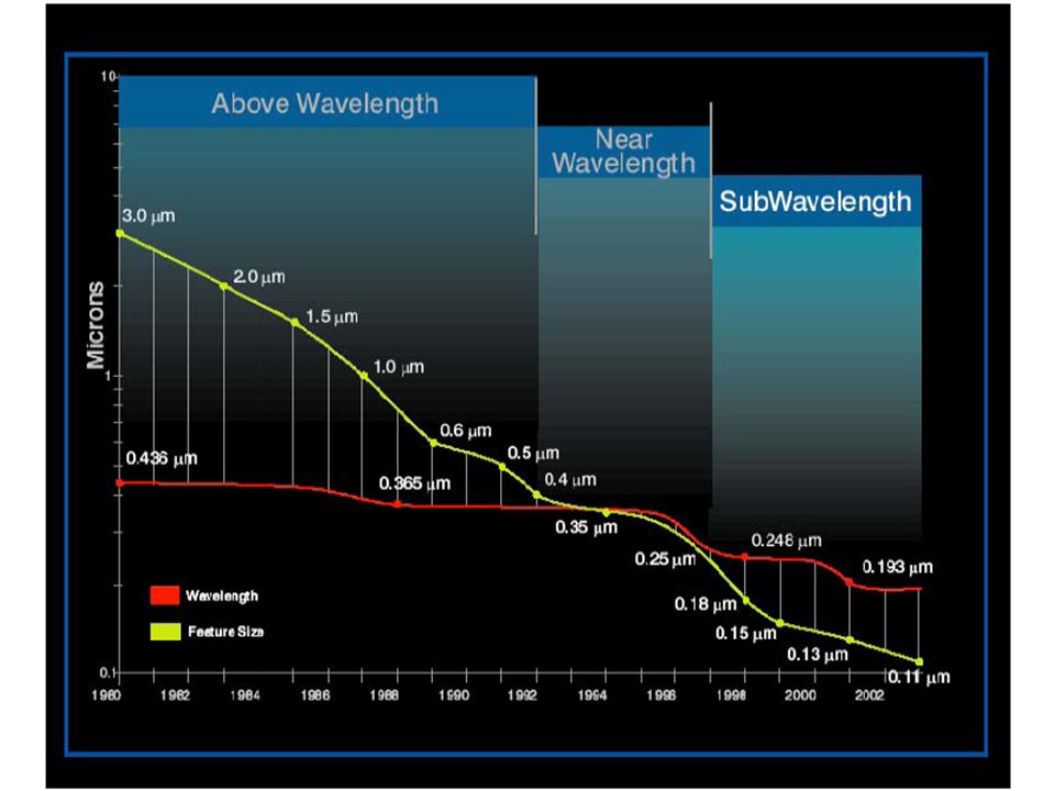
7
Subwavelength Lithography Challenges Source: Raul Camposano, 2003

8
The Designer’s Escalating Problem Source: Raul Camposano, 2003

9
Wire Delays and Noise Problems Dramatically Complicate Design Unstructured “Place and Route” Standard Cell Methodologies will Breakdown 1 cycle180 nm 45 nm

10
ASIC NRE Costs Not Justified for Many Applications Forecast: By 2010, a complex ASIC will have an NRE Cost of over $40M = $28M (NRE Design Cost) + $12M (NRE Mask Cost) Many “ASIC” applications will not have the volume to justify a $40M NRE cost e.g. a $30 IC with a 33% margin would require sales of 4M units (x $10 profit/IC) just to recoup $40M NRE Cost
 just to recoup $40M NRE Cost.")
11
Case For Programmable Solutions Can “amortized” high NRE costs across many applications – e.g. microprocessors, DSPs, FPGAs Complex ASICs today require 18+ months vs. ~4 months for same function on DSP – e.g. Voice-over-IP chip vs. Voice-over-IP on a DSP – “Design time” gap will widen dramatically Many applications simply requires “programmability”, e.g. cell phones – multiple modes – evolving standards – evolving features, differentiation …

12
But … Advance applications and algorithms (e.g. latest video games, broadband wireless …) require enormous computation power – 100s to 1000s of GOPS And very high efficiency – 100s of MOPS/mW (GOPS/W) – 10s of GOPs/$ Existing microprocessors, DSPs, and FPGAs don’t come close
 require enormous computation power – 100s to 1000s of GOPS And very high efficiency – 100s of MOPS/mW (GOPS/W) – 10s of GOPs/$ Existing microprocessors, DSPs, and FPGAs don’t come close.")
13
Why are Conventional Processor Architectures Inefficient? e.g. Intel Itanium II – 6-Way Integer Unit < 2% die area – Cache logic > 50% die area Most of chip there to keep these 6 Integer Units at “peak” rate Main issue is external DRAM latency (50ns) to internal clock (0.25ns) is 200:1 Can “in theory” fit >300 ALUs (tens of thousands in future) in same die area, but how to keep them “busy”? INT6 Cache logic
 to internal clock (0.25ns) is 200:1 Can in theory fit >300 ALUs (tens of thousands in future) in same die area, but how to keep them busy . INT6 Cache logic.")
14
Why are ASICs so Efficient? Parallelism (Millions of gates operating in parallel) Locality (Fed by dedicated “local” wires & memories) Source: Bill Dally, 2003
 Locality (Fed by dedicated local wires & memories) Source: Bill Dally,")
15
20MIPS cpu in 1987 Few thousand gates Source: Anant Agarwal, MIT, NOCS 2009 Keynote

16
The billion transistor chip of 2007 Source: Anant Agarwal, MIT, NOCS 2009 Keynote

17
Tilera’s TILEPro64™ Processor Power per tile (depending on app)170 – 300 mW Core power for h.264 encode (64 tiles) 12W Clock speed Up to 866 MHz I/O bandwidth40 Gbps Main Memory bandwidth200 Gbps Multicore Performance (90nm) Number of tiles64 Cache-coherent distributed cache5 MB Operations @ 750MHz (32, 16, 8 bit)144-192-384 BOPS Bisection bandwidth2 Terabits per second Power Efficiency I/O and Memory Bandwidth Programming ANSI standard C SMP Linux programming Stream programming Product reality Source: Anant Agarwal, MIT, NOCS 2009 Keynote
170 – 300 mW Core power for h.264 encode (64 tiles) 12W Clock speed Up to 866 MHz I/O bandwidth40 Gbps Main Memory bandwidth200 Gbps Multicore Performance (90nm) Number of tiles64 Cache-coherent distributed cache5 MB 750MHz (32, 16, 8 bit) BOPS Bisection bandwidth2 Terabits per second Power Efficiency I/O and Memory Bandwidth Programming ANSI standard C SMP Linux programming Stream programming Product reality Source: Anant Agarwal, MIT, NOCS 2009 Keynote")
18
PCIe 1 MAC PHY PCIe 1 MAC PHY PCIe 0 MAC PHY PCIe 0 MAC PHY Serdes Flexible IO GbE 0 GbE 1 Flexible IO UART, HPI JTAG, I2C, SPI UART, HPI JTAG, I2C, SPI DDR2 Memory Controller 3 DDR2 Memory Controller 0 DDR2 Memory Controller 2 DDR2 Memory Controller 1 XAUI MAC PHY 0 XAUI MAC PHY 0 Serdes XAUI MAC PHY 1 XAUI MAC PHY 1 Serdes Tile Processor Block Diagram A Complete System on a Chip PROCESSOR P2 Reg File P1P0 CACHE L2 CACHE L1IL1D ITLBDTLB 2D DMA STN MDNTDN UDNIDN SWITCH Source: Anant Agarwal, MIT, NOCS 2009 Keynote

19
What Does the Future Look Like? Corollary of Moore’s law: Number of cores will double every 18 months ‘05‘08‘11‘14 6425610244096 ‘02 16 Research Industry 16642561024 4 (Cores minimally big enough to run a self respecting OS!) 1K cores by 2014! Are we ready? Source: Anant Agarwal, MIT, NOCS 2009 Keynote
 1K cores by Are we ready. Source: Anant Agarwal, MIT, NOCS 2009 Keynote.")
20
Massively Parallel Processing On-a-Chip 2 GB/s 544 GB/s Registers SRAM 32 GB/s DDR Interface 64 Tiles x 8 ALUs = 512 ALUs @ 2 GHz, 1000 GOPS = 1 TOPS Parallelism + Locality DDR DRAM Bandwidth Hierarchy is Key Source: Bill Dally, 2003

21
IBM/Sony/Toshiba Cell Processor Used in Playstation 3 4.6 GHz 64-bit Dual-Threaded PowerPC 8 SIMD Engines x 7 ALUs = 56 ALUs @ 4.6 GHz = 256 GFLOPS Terabit on-chip ring network Terabit external memory and chip-to-chip IO 90nm process 234 million transistors 221 mm 2 die 0.5 Tb/s Memory I/O 0.5 Tb/s Chip I/O SIMD Engine 7 ALUs 64-bit Dual-Thread PowerPC Tb/s Ring Network

22
NVIDIA GeForce 8800 8 Clusters x 16 ALUs = 128 ALUs 32-bit on-chip CPU Terabit external memory IO 1.35 GHz clock 90nm process 681 million transistors 32-bit CPU 0.7 Tb/s Memory I/O 8 clusters x 16 ALUs = 128 ALUs

Similar presentations


![EE314 Basic EE II Silicon Technology [Adapted from Rabaey’s Digital Integrated Circuits, ©2002, J. Rabaey et al.]](/16/5137281/big_thumb.jpg "EE314 Basic EE II Silicon Technology [Adapted from Rabaey’s Digital Integrated Circuits, ©2002, J. Rabaey et al.]>")


