Download presentation
Presentation is loading. Please wait.

1
Ch 8. Sequential logic design practices 1. Documentation standards ▶ general requirements : signal name, logic symbol, schematic logic - state machine layout : a collection of F/F & combination logic on same - flip-flops : type, function, clocking behavior - state machine description : state table/diagram, transition list text files in H/W description language (VHDL) - Cascaded elements. - timing diagrams - timing spec : max.clock freq, set-up & hold time min. pulse width
 - Cascaded elements. - timing diagrams - timing spec : max.clock freq, set-up & hold time min. pulse width.")
2
8.1.4 Timing Diagrams and Specification setup time margin = t clk – t ffpd(max) – t comb(max) – t setup hold time margin = t ffpd(min) + t comb(min) + t hold
 – t comb(max) – t setup hold time margin = t ffpd(min) + t comb(min) + t hold")
3
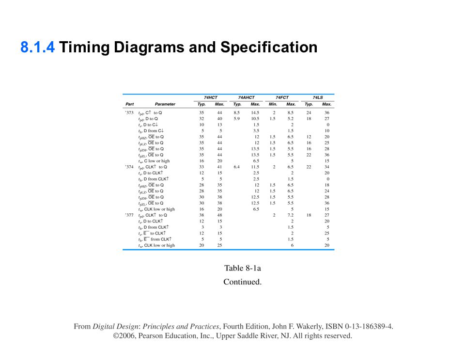
Propagation delay in ns of selected CMOS flip-flops, registers, and latches 8.1.4 Timing Diagrams and Specification

6
2. Latch & flip flops 8.2.1 SSI Latches and flip flops

7
8.2.2 Switch debouncing

8
8.2.3 The Simplest Switch debounder

10
8.2.4 Bus Holder Circuit Low & high -> floating Low high Source or sink a small amount of additional current through R If pull-up resistor is too high, slow transition If pull-up resistor is too low, too much current

11
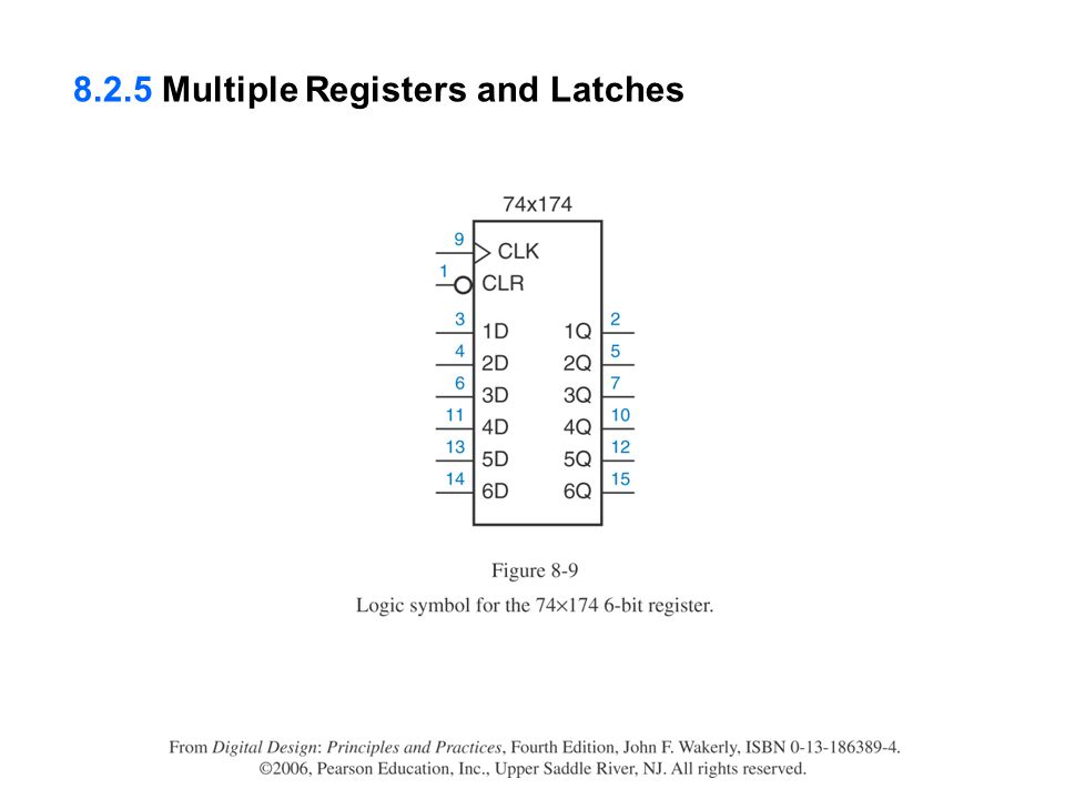
8.2.5 Multiple Registers and Latches

16
If EN_L = 1, Q <- Q If EN_L = 0, Q <- P

17
8.2.6 Registers and Latches in ABEL and PLDs Data1 in Rom is read Data2 in a different device is read

18
8.2.6 Registers and Latches in ABEL and PLDs

20
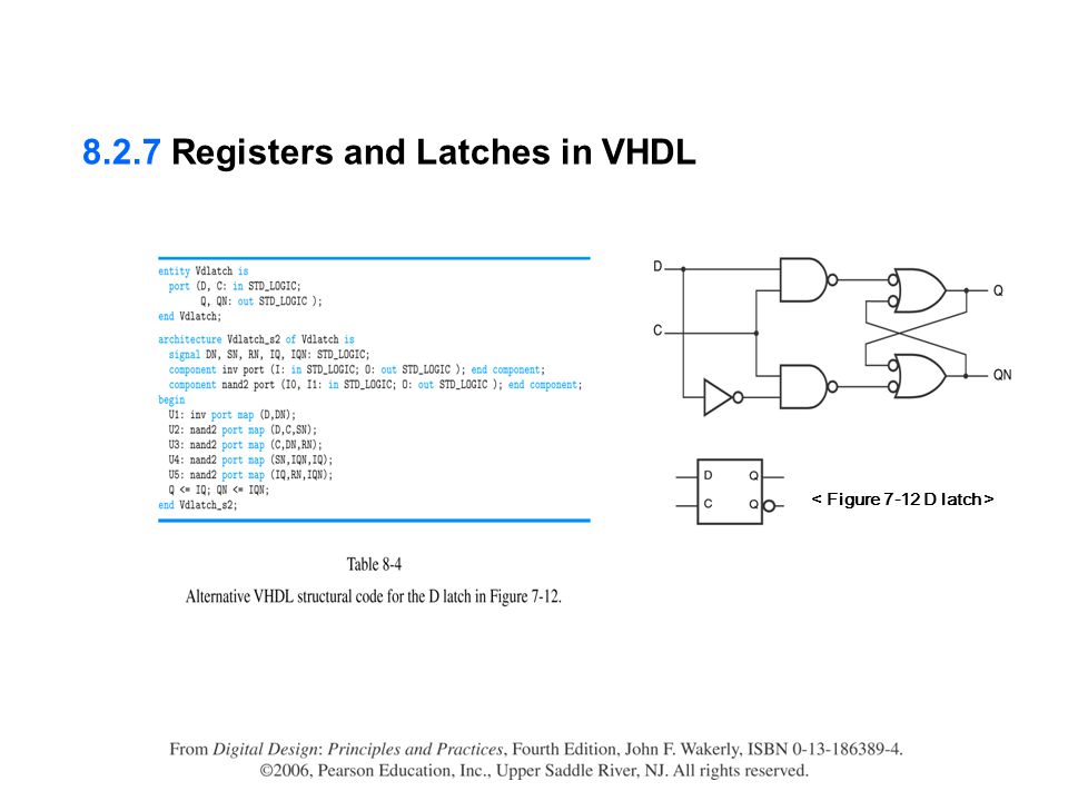
8.2.7 Registers and Latches in VHDL

22
8.2.7 Registers and Latches in VHDL - Inferred latch - The code doesn’t say what to do if C ≠ 1, - The compiler infers a latch to retain the value of Q

23
8.2.7 Registers and Latches in VHDL

25
8.2.7 Registers and Latches in VHDL

26
3. Sequential PLD 8.3.1 Sequential GAL Devices

28
-No architecture control bits -More product terms 8-16 terms -Two more inputs

29
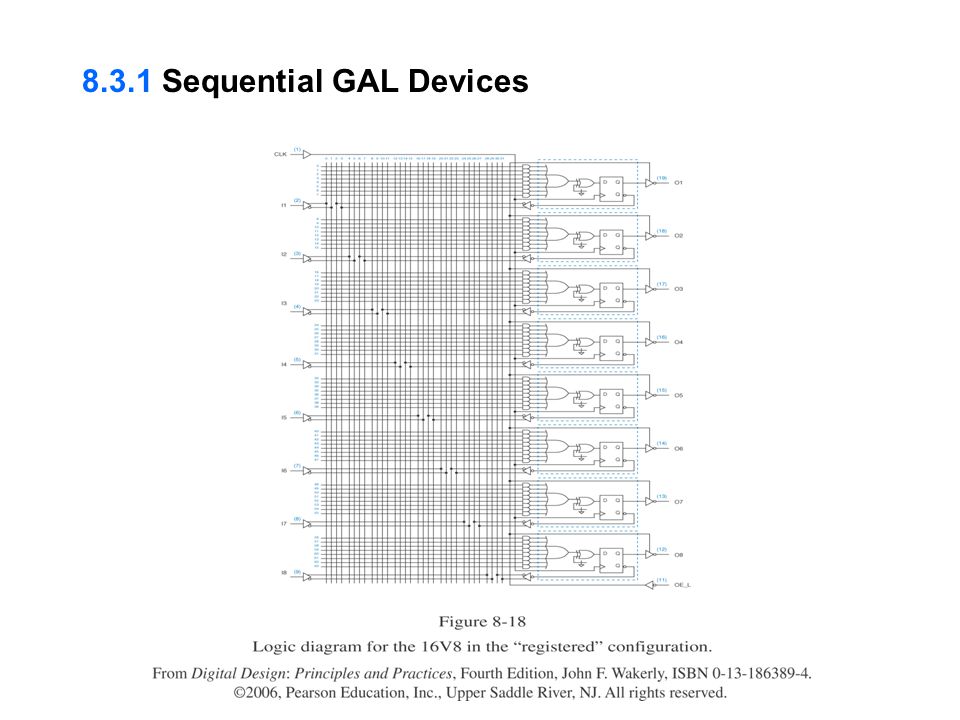
8.3.1 Sequential GAL Devices

31
8.3.2 PLD Timing Specification ㆍ A series PLD (ex : PAL26L8A ) : t PD = 25n, t CO =15n, t SU = 25 nsec ㆍ Suffix : -5, -7, A, B,…
 : t PD = 25n, t CO =15n, t SU = 25 nsec ㆍ Suffix : -5, -7, A, B,…")
32
8.3.2 PLD Timing Specification ㆍ t PD : propagation delay from input to output ㆍ t CO : P-delay from rising edge of clock to output ㆍ t SU (set-up), t cf ( = t CO ), t H ( hold) f max : reliable max.freq ㆍ external PLD : PLD output -> connect to input of another PLD ㆍ internal PLD : same PLD
, t cf ( = t CO ), t H ( hold) f max : reliable max.freq ㆍ external PLD : PLD output -> connect to input of another PLD ㆍ internal PLD : same PLD")
33
4. Counters state diagram = single cycles

34
Ripple counter ㆍ connect in series or cascaded f/f ㆍ Carry : ripples from LSB to MSB one bit at a time ㆍ slow : n * t PTQ ( propagation delay of T f/f) CLK : applied to LSB F/F only 8.4.1 Ripple Counters
 CLK : applied to LSB F/F only Ripple Counters")
35
8.4.2 Synchronous Counters

37
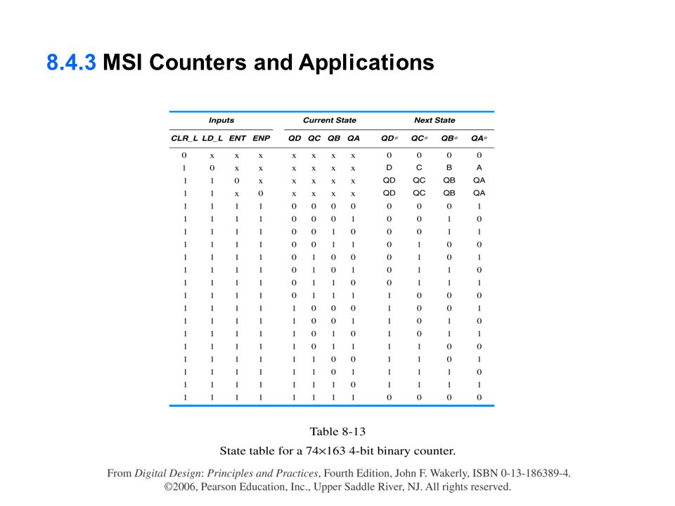
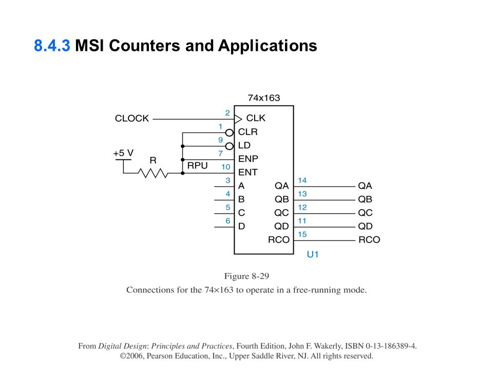
- MSI counter : Modulus N counter/divider i) Sync : ㆍ binary 4 bit counter ( 161,163 ) 161 : Async. clear function 163 : Sync. clear ( fully sync. counter ) ㆍ decade counter : 160, 162 ex) modulo-10 counter wavefarm ㆍ 4 bit up/down counter : SN74169(TTL), 74C169(CMOS), CD40169(CMOS) up/down decade counter : 192 ii ) Async : ㆍ 4 bit binary counter : 193 ㆍ 12 counter : 92 ㆍ decade counter : 90 ㆍ 4 bit up/down counter : 191 ㆍ decade up/down counter : 190 8.4.3 MSI Counters and Applications
 ㆍ decade counter : 160, 162 ex) modulo-10 counter wavefarm ㆍ 4 bit up/down counter : SN74169(TTL), 74C169(CMOS), CD40169(CMOS) up/down decade counter : 192 ii ) Async : ㆍ 4 bit binary counter : 193 ㆍ 12 counter : 92 ㆍ decade counter : 90 ㆍ 4 bit up/down counter : 191 ㆍ decade up/down counter : MSI Counters and Applications.")
40
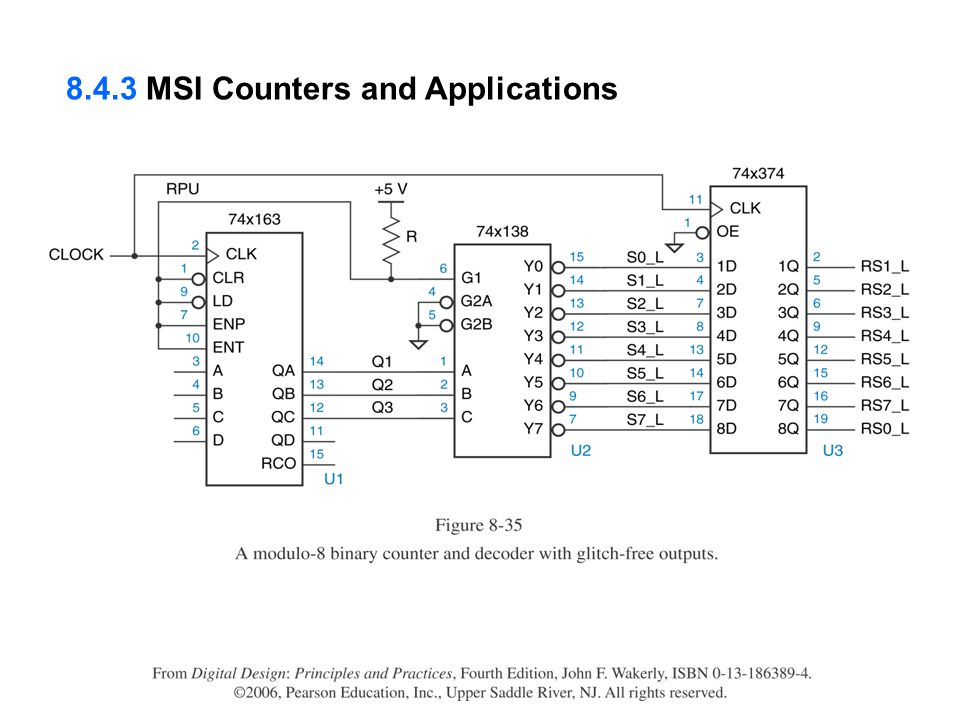
RCO = 1 when OA = OB = OC = OD = 1 & ENT = 1 8.4.3 MSI Counters and Applications

48
8.4.6 Counters in VHDL

53
5. Shift Register 8.5.1 Shift Register Structure

55
8.5.2 MSI Shift Register

57
ㆍ 4 bit bidirectional parallel-in, parallel-out shift register = universal shift register ( shift left & right, parallel & serial in-out combination ) ㆍ left ( Q D -> Q A ) & right ( Q A -> Q D ) Rin ( right – in ) & Lin ( left – in ) 8.5.2 MSI Shift Register
 ㆍ left ( Q D -> Q A ) & right ( Q A -> Q D ) Rin ( right – in ) & Lin ( left – in ) MSI Shift Register")
58
8.5.3 Shift Register Counters

59
S1S0 = 10 RESET = 1, 0001 load then RESET = Ø = SØ 8.5.3 Shift Register Counters

61
8.5.4 Ring Counters

62
If Q0, Q1, Q2=1, then Ø to LIN If Q0, Q1, Q2=0, then 1 to LIN 8.5.4 Ring Counters

64
If Q0, Q1, Q2=1, LIN = Ø Else LIN = 1 when RESET, 1110 load 8.5.4 Ring Counters

65
RESET = Ø = CLR, Q3Q2Q1Q0 = 0000 If Q3 = Ø, LIN = 1 If Q3 = 1, LIN = Ø 8.5.4 Ring Counters

66
8.5.5 Johnson Counters

67
DQDQDQ CLK Q : Twisted ring counter 2n : 1 scalar Ex) if n=4, 8 states Simple decoding logic Ex) 4 bit Johnson counter [ ref binary counter ] 8.5.5 Johnson Counters
![DQDQDQ CLK Q : Twisted ring counter 2n : 1 scalar Ex) if n=4, 8 states Simple decoding logic Ex) 4 bit Johnson counter [ ref binary counter ] Johnson Counters](http://images.slideplayer.com/13/3943956/slides/slide_67.jpg "DQDQDQ CLK Q : Twisted ring counter 2n : 1 scalar Ex) if n=4, 8 states Simple decoding logic Ex) 4 bit Johnson counter [ ref binary counter ] Johnson Counters")
68
2 n – 2n abnormal states OXXO -> 0001 Then LOAD 0001 N = 4, 2 4 – 2x4 = 8 (abnormal states) If Q3 = 0, LIN = 1 If Q3 = 1, LIN = Ø 8.5.5 Johnson Counters
 If Q3 = 0, LIN = 1 If Q3 = 1, LIN = Ø Johnson Counters")
69
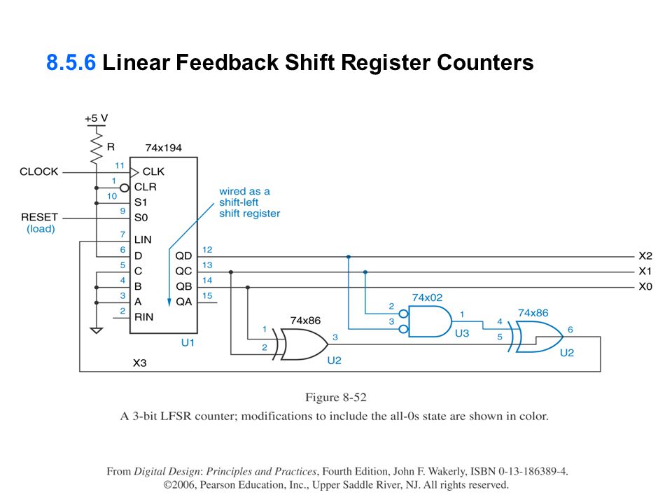
8.5.6 Linear Feedback Shift Register Counters

73
8.5.7 Shift Register in ABEL and PLDs

74
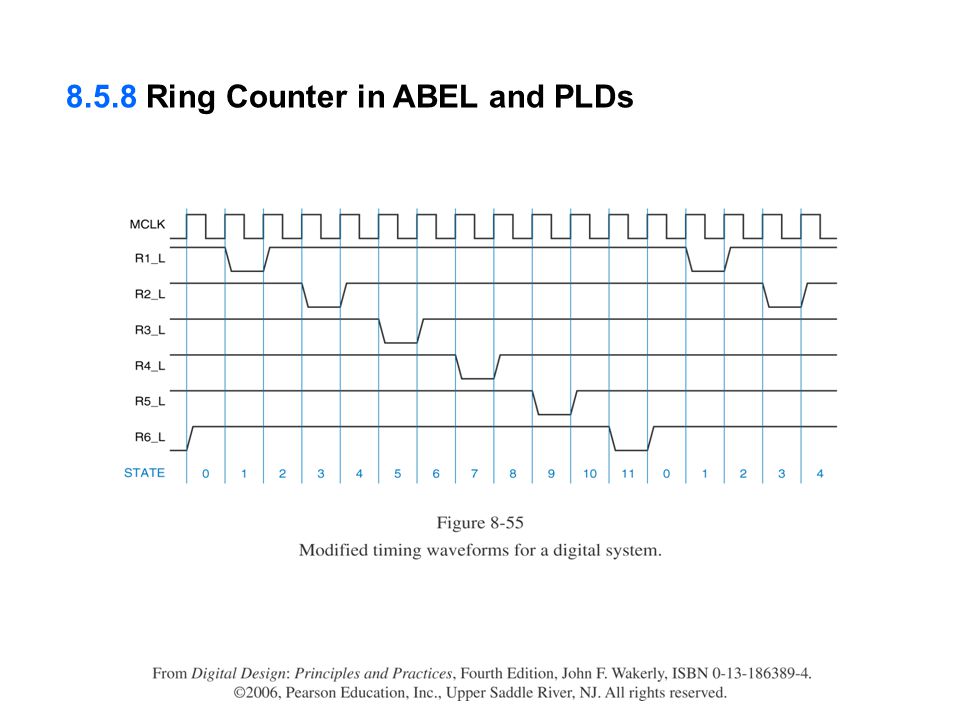
8.5.8 Ring Counter in ABEL and PLDs

76
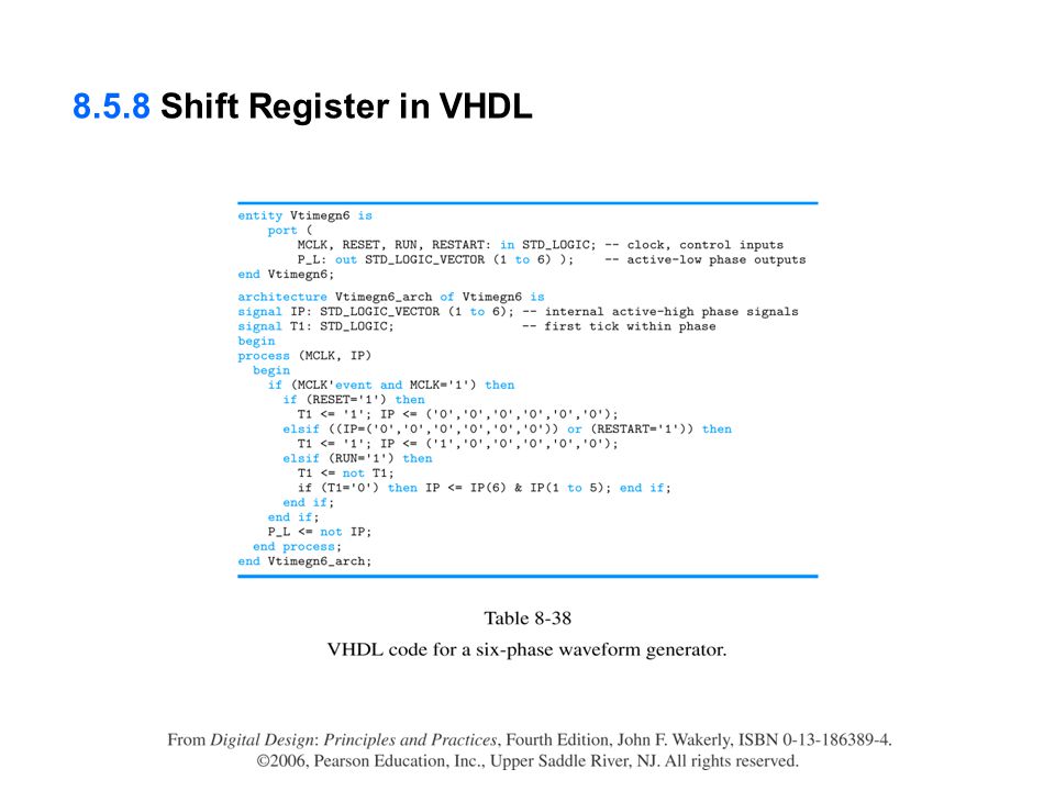
8.5.8 Shift Register in VHDL

81
6. Iterative versus Sequential Circuits

82
If X = Y, A = 1, EQI = 1, -> then EQO = 1 If X ≠ Y, A = 0, EQI = 1, -> then EQO = Ø

84
RESET_L = Ø EQO = 1, next clock EQI = 1

86
design goal for the digital systems ⅰ ) function as required ⅱ ) high reliable & easy maintenance ⅲ ) cost effective design factor for the reliable digital systems clock skew & gating the clock static, dynamic, function hazards 7. Synchronous Design Methodology

87
8.7.1 Synchronous System Structure

89
▶ design factor for reliable digital systems ⅰ ) clock skew ⅱ ) gating the clock 1) clock skew difference between arrival times (of a clock at different devices) - for proper operation t ffpd(min) + t comg(min) - t hold – t skew(max) > 0 if hold time margin > clock skew, then system → OK 8. Impediments to Synchronous Design

90
8.8.1 Clock Skew

94
8.8.2 Gating the Clock

95
If CLKEN = Ø, GCLK = 1 (not ticking) If CLKEN = 1, GCLK = Clock_L = Clock 8.8.2 Gating the Clock
 If CLKEN = 1, GCLK = Clock_L = Clock Gating the Clock")
96
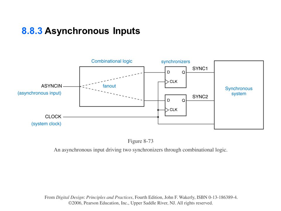
8.8.3 Asynchronous Inputs

100
▶ metastable : Set-up & hold time → violation (not meet) ▶ Synchronizer failure - if system → use synchronizer output, while output → metastable output solution ⅰ ) min. pulse width, set-up time ⅱ ) wait “ long enough” until f/f → come out of metastable ▶ metastability resolution time : t r t r = t clk – t comb – t setup ▶ reliable synchronous design ⅰ ) wait “long enough” → slow down ⅱ ) for speed up use 9. Synchronizer Failure and Metastability
 wait long enough until f/f → come out of metastable ▶ metastability resolution time : t r t r = t clk – t comb – t setup ▶ reliable synchronous design ⅰ ) wait long enough → slow down ⅱ ) for speed up use 9. Synchronizer Failure and Metastability.")
101
8.9.1 Synchronizer Failure

102
8.9.3 Reliable Synchronizer Design

104
8.9.5 Better Synchronizers

106
8.9.6 Other Synchronizer Designs

108
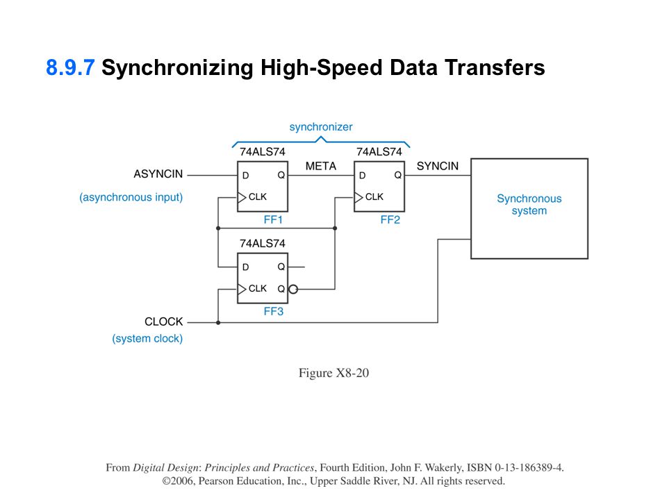
8.9.7 Synchronizing High-Speed Data Transfers

Similar presentations


 in addition to its current inputs The state of the circuit is.>")


>")


