Download presentation
Presentation is loading. Please wait.

1
8253/54 Timer Section 5.1 8253/54 Timer Description and Initialization
PTI (programmable Interval Timer) The 8253 chip was used in the IBM PC/XT, but starting with the IBM PC/AT, the 8254 replaced the 8253. 8253 and 8254 have exactly the same pinout. 8254 is a superset of the 8253.
 The 8253 chip was used in the IBM PC/XT, but starting with the IBM PC/AT, the 8254 replaced the and 8254 have exactly the same pinout is a superset of the")
2
Programmable Interval Timer - 8254

5
Pin Description of 8253/54 A0, A1, and CS
Inside the 8253/54 timer, there are 3 counters. Each timer works independently and programmed separately. Each counter is assigned an individual port address. The control register common to all 3 counters and has its own port.

7
CLK CLK is the input clock frequency, which can range between 0 and 2 MHz for the 8253. For input frequencies higher than 2 MHz, the 8254 must be used. The 8254 can go as high as 8 MHz, and can go 10 MHz. OUT Can have square-wave, one-shot, and other square-shape waves for various duty cycles but no sine-wave or saw-tooth shapes. Gate This pin is used to enable or disable the counter.

8
D0-D7 The D0-D7 data bus of the 8253/54 is a bidirectional bus connected to D0-D7 of the system data bus. RD and WR are connected to IOR and IOW control signals of the system bus. Initialization of the 8253/54 Each of the three counters of the 8253/54 must be programmed separately. The 8253/54 must be initialized before it is used.

13
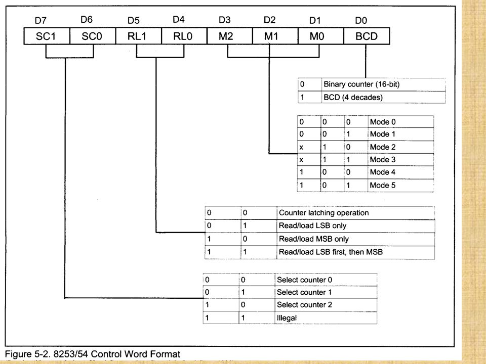
Control word The figure shows the one-byte control word of the 8253/54. D0 chooses between a binary number divisor of 0000 to FFFFH or a BCD divisor of 0000 to 9999H. The highest number is 216 for binary and 104 for BCD. To get the highest count, the counter is loaded with zeros. D1, D2, and D3 are for mode selection.

14
D4 and D5 are for RL0 and RL1 RL0 and RL1 are used to indicate the size of the divisor, and have 3 options: Read/write MSB only Read/write LSB only Read/write LSB first followed immediately by the MSB.

15
Operation Modes Mode 0 Interrupt on terminal count
Mode 1 Programmable one-shot Mode 2 Rate Generator Mode 3 Square wave rate generator Mode 4 Software triggered strobe Mode 5 Hardware trigger strobe

16
All counters are down counters.
D6 and D7 are used to select the 3 counters, counter 0, counter 1, or counter 2, is to be initialized by the control byte. To program a given counter of the 8253/54 to divide the CLK input frequency one must send the divisor to that specific counter’s reg. To divide the frequency by (BCD) or (binary) we must send in 0 for both high and low bytes.
 or (binary) we must send in 0 for both high and low bytes.")
Similar presentations


 Data Sheet Machine Projects –Continue on MP3 Labs –Continue in labs with your assigned.>")

, No Bidirectional.>")


 Read-Write Memory (RAM)>")


