Download presentation
Presentation is loading. Please wait.

1
Architecture and Instruction Set of the C6x Processor Module 1

3
Reference R. Chassaing, DSP applications using C and the TMS 320C6x DSK, Wiley, 2002

4
DSP TMS320 Introduction Architecture Functional Unit Fetch & Execute Packet Pipelining Registers Addressing Modes

5
DSP Digital Signal Processing : Application of mathematical operations to digitally represented signal Signals represented digitally as sequence of samples. Digital Signal Processor: Electronics System that process digital Signal.

6
DSP System

7
DSP tasks Most DSP tasks Require – Repetitive numeric computation – Real time processing – High memory – System flexibility DSP must perform these tasks efficiently while minimizing – Cost – Power – Memory use – Development time

8
TMS DSP IC TMS 320 C6X – TMX – experimental device – TMP – prototype – TMS – Qualified device – 320- TI DSP family – C- CMOS with ROM – E- CMOS with EPROM – 5- Generation – X- version number

9
TMS320 Introduction Texas Instruments introduced the first generation TMS32010 digital signal processor in 1982, the TMS320C25 in 1986, and the TMS320C50 in 1991. These 16-bit processors are all fixed pointprocessors and are code-compatible.

10
Von neumann VS Harvard The fixed-point processors C1x, C2x, and C5x are based on a modified Harvard architecture with separate memory spaces for data and instructions that allow concurrent accesses. Quantization error or round-off noise from an ADC is a concern with a fixed point processor.

11
The TMS320C30 floating-point processor was introduced in the late 1980s. The TMS320C6201 (C62x), announced in 1997. C62x is based on a very-long-instruction-word (VLIW) architecture, still using separate memory spaces for instructions and data as with the Harvard architecture. The C62x is not code-compatible with the previous generation of fixed-point processors.
, announced in C62x is based on a very-long-instruction-word (VLIW) architecture, still using separate memory spaces for instructions and data as with the Harvard architecture. The C62x is not code-compatible with the previous generation of fixed-point processors..")
13
TMS320C6x ARCHITECTURE The TMS320C6711 is a floating-point processor based on the VLIW architecture. Internal memory includes a two-level cache architecture with 4kB of level 1 program cache (L1P), 4kB of level 1 data cache (L1D), and 64kB of RAM or level 2 cache for data/program allocation (L2). It has a direct interface to both synchronous memories and asynchronous memories
, 4kB of level 1 data cache (L1D), and 64kB of RAM or level 2 cache for data/program allocation (L2). It has a direct interface to both synchronous memories and asynchronous memories.")
14
On-chip peripherals include two multichannel buffered serial ports (McBSPs),two timers, a 16-bit host port interface (HPI), and a 32-bit external memory interface (EMIF). It requires 3.3V for I/O and 1.8V for the core (internal). Internal buses – 32-bit program address bus – 256-bit program data bus (eight 32-bit instructions), – two 32-bit data address buses, – two 64-bit data buses – two 64-bit store data buses. With a 32-bit address bus, the total memory space is 2^32 = 4GB, including four external memory spaces: CE0, CE1, CE2, and CE3.
. Internal buses – 32-bit program address bus – 256-bit program data bus (eight 32-bit instructions), – two 32-bit data address buses, – two 64-bit data buses – two 64-bit store data buses. With a 32-bit address bus, the total memory space is 2^32 = 4GB, including four external memory spaces: CE0, CE1, CE2, and CE3..")
15
3-Access level of Memory Map 1. L1 Memory -Cache-based Architecture -Program Cache & Data Cache -Size : PC(4Kbyte), DC(4Kbyte) 2. L2 Memory - Size : 64Kbyte - Program & Data 3. L3 Memory External Memory
, DC(4Kbyte) 2. L2 Memory - Size : 64Kbyte - Program & Data 3. L3 Memory External Memory.")
16
Internal Memory

18
Independent memory banks on the C6x allow for two memory accesses within one instruction cycle. Two independent memory banks can be accessed using two independent buses. Two loads or two stores instructions can be performed in parallel. No conflict results if the data accessed are in different memory banks. Separate buses for program, data, and direct memory access (DMA) allow the C6x to perform concurrent program fetches, data read and write, and DMA operations.
 allow the C6x to perform concurrent program fetches, data read and write, and DMA operations..")
19
C6x has a byte-addressable memory space. Internal memory is organized as separate program and data memory spaces, with two 32- bit internal ports (two 64-bit ports with the C64x) to access internal memory. With a clock of 150MHz onboard the DSK, one can ideally achieve two multiplies and accumulates per cycle, for a total of 300 million multiplies and accumulates (MACs) per second.
 to access internal memory. With a clock of 150MHz onboard the DSK, one can ideally achieve two multiplies and accumulates per cycle, for a total of 300 million multiplies and accumulates (MACs) per second..")
20
With six of the eight functional units capable of handling floating-point operations, it is possible to perform 900 million floating-point operations per second (MFLOPS). 1200 million instructions per second (MIPS)
.")
21
FUNCTIONAL UNITS The CPU consists of eight independent functional units divided into two data paths Each path has a unit for – multiply operations (.M), – logical and arithmetic operations (.L), – branch, bit manipulation, and arithmetic operations (.S), – loading/storing and arithmetic operations (.D). The.S and.L units are for arithmetic, logical, and branch instructions. All data transfers make use of the.D units.

23
The arithmetic operations, such as subtract or add (SUB or ADD), can be performed by all the units except the.M units. The eight functional units consist of four floating/fixed-point ALUs (two.L and two.S), two fixed-point ALUs (.D units), and two floating/fixed-point multipliers (.M units).
, two fixed-point ALUs (.D units), and two floating/fixed-point multipliers (.M units)..")
24
Each path includes a set of sixteen 32-bit registers, A0 through A15 and B0 through B15. Two cross-paths (1x and 2x) allow functional units from one data path to access a 32-bit operand from the register file on the opposite side. Each functional unit side can access data from the registers on the opposite side using a cross-path. There are 32 general purpose registers, but some of them are reserved for specific addressing or are used for conditional instructions.
 allow functional units from one data path to access a 32-bit operand from the register file on the opposite side. Each functional unit side can access data from the registers on the opposite side using a cross-path. There are 32 general purpose registers, but some of them are reserved for specific addressing or are used for conditional instructions..")
25
VelociTI ™ VLIW modification done by TI is called VelociTI – Reduces code size – Increases performance when instructions reside off-chip C6X architecture is based on the high-performance advanced VelociTI very-long-instruction-word (VLIW) architecture developed by Texas Instruments (TI) an excellent choice for multichannel and multifunction applications (Several instructions captured & processed simultaneously)
 architecture developed by Texas Instruments (TI) an excellent choice for multichannel and multifunction applications (Several instructions captured & processed simultaneously)")
26
VelociTI ™ VLIW modification done by TI is called VelociTI – Reduces code size – Increases performance when instructions reside off-chip C6X architecture is based on the high-performance advanced VelociTI very-long-instruction-word (VLIW) architecture developed by Texas Instruments (TI) an excellent choice for multichannel and multifunction applications (Several instructions captured & processed simultaneously)
 architecture developed by Texas Instruments (TI) an excellent choice for multichannel and multifunction applications (Several instructions captured & processed simultaneously)")
27
FETCH AND EXECUTE PACKETS The architecture VELOCITI, introduced by TI, is derived from the VLIW architecture. An execute packet (EP) consists of a group of instructions that can be executed in parallel within the same cycle time. The number of EPs within a fetch packet (FP) can vary from one to eight The VLIW architecture was modified to allow more than one EP to be included within an FP.
 consists of a group of instructions that can be executed in parallel within the same cycle time. The number of EPs within a fetch packet (FP) can vary from one to eight The VLIW architecture was modified to allow more than one EP to be included within an FP..")
28
The least significant bit of every 32-bit instruction is used to determine if the next or subsequent instruction belongs in the same EP (if 1) or is part of the next EP if 0).
 or is part of the next EP if 0).")
29
EP1 contains the two parallel instructions A and B; EP2 contains the three parallel instructions C, D, and E; and EP3 contains the three parallel instructions F, G, and H. Bit 0 (LSB) of each 32-bit instruction contains a “p” bit that signals whether it is in parallel with a subsequent instruction. The “p” bit of instruction B is zero, denoting that it is not within the same EP as the subsequent instruction C. Similarly, instruction E is not within the same EP as instruction F.
 of each 32-bit instruction contains a p bit that signals whether it is in parallel with a subsequent instruction. The p bit of instruction B is zero, denoting that it is not within the same EP as the subsequent instruction C. Similarly, instruction E is not within the same EP as instruction F..")
30
Pipelining Pipelining is a key feature in a digital signal processor to get parallel instructions working properly. There are three stages of pipelining: – program fetch, decode, and execute.

31
non-pipelined scalar architecture - A processor that executes every instruction one after the other - may use processor resources inefficiently, potentially leading to poor performance. pipelining - executing different sub-steps of sequential instructions simultaneously superscalar architectures - executing multiple instructions entirely simultaneously

33
Pipelining does not decrease the time for individual instruction execution. Instead, it increases instruction throughput. The throughput of the instruction pipeline is determined by how often an instruction exits the pipeline If the stages are perfectly balanced, then the time per instruction on the pipelined machine is equal to Time per instruction on nonpipelined machine Number of pipe stages

34
Program Fetch The program fetch stage is composed of four phases: (a) PG: program address generate (in the CPU) to fetch an address (b) PS: program address send (to memory) to send the address (c) PW: program address ready wait (memory read) to wait for data (d) PR: program fetch packet receive (at the CPU) to read opcode from memory
 PG: program address generate (in the CPU) to fetch an address (b) PS: program address send (to memory) to send the address (c) PW: program address ready wait (memory read) to wait for data (d) PR: program fetch packet receive (at the CPU) to read opcode from memory")
36
Decode Stage The decode stage is composed of two phases: (a) DP: to dispatch all the instructions within an FP to the appropriate functional units (b) DC: instruction decode
 DP: to dispatch all the instructions within an FP to the appropriate functional units (b) DC: instruction decode")
37
Execute Stage The execute stage is composed of from six phases (with fixed point) to 10 phases (with floating point), due to delays (latencies) associated with following instructions: (a) Multiply instruction, which consists of two phases due to one delay (b) Load instruction, which consists of five phases due to four delays (c) Branch instruction, which consists of six phases due to five delays
 to 10 phases (with floating point), due to delays (latencies) associated with following instructions: (a) Multiply instruction, which consists of two phases due to one delay (b) Load instruction, which consists of five phases due to four delays (c) Branch instruction, which consists of six phases due to five delays")
38
Pipeline phases Program fetchdecode execute PG PS PW PRDP DC E1- E6 ( E1-E10 for double precision) Pipelining effects Clock cycles 123456789101112 PGPSPWPRDPDCE1E2E3E4E5E6 PGPSPWPRDPDCE1E2E3E4
 Pipelining effects Clock cycles PGPSPWPRDPDCE1E2E3E4E5E6 PGPSPWPRDPDCE1E2E3E4")
39
Each row represents an FP PG of first FP starts in cycle 1,PG of second FP starts in cycle 2 and so on…. Each FP has 4 phases for fetch,2 phases for decode and execution phases can take from 1 to 10 phases At cycle 7, instruction in the first FP are in the first execution phase E1, instruction in the second FP is in decoding phase, instruction in the third FP is in dispatching phase and so on….. All the instructions are proceeding through various phases Therefore pipeline is FULL

40
Most instructions have 1 execute phase Multiply (MPY) has 2 Load (LDH/LDW) has 5 Branch (B) has 6 phases Additional execute phases are associated with floating point and double precision type instructions (upto 10 phases) eg: MPYDP has 9 delay slots and a total 10 phases Functional unit latency: The number of cycles that an instruction ties up a functional unit. it is 1 for all instructions except double precision instructions no other instructions can use the functional unit it is different from delay slot eg: MPYDP has 4 functional unit latency but 9 delay slots delay slot: some instructions that are physically after the instruction are executed as if they were located before it. Classic examples are branch and call instructions, which often execute the following instruction before the branch or call is performed.

41
Registers – The two register files each contain 16 32-bit registers for a total of 32 general-purpose registers (A 0 ~A 15, B 0 ~B 15 ) – Interaction with the CPU must be done through these registers – The four functional units on each side of the CPU can freely share the 16 registers belonging to that side. – two cross paths 1x and 2x connects all the registers on the other side – (which can access data from the register files on the opposite side.) – If register access is by functional units on the same side of the CPU, register file can service all the units in a single clock cycle
 – If register access is by functional units on the same side of the CPU, register file can service all the units in a single clock cycle.")
42
Registers A0, A1, B0, B1 are used as conditional registers. Registers A4 through A7 and B4 through B7 are used for circular addressing. Registers A0 through A9 and B0 through B9 (except B3) are temporary registers. Any of the registers A10 through A15 and B10 through B15 used fsubroutine.
 are temporary registers. Any of the registers A10 through A15 and B10 through B15 used fsubroutine..")
43
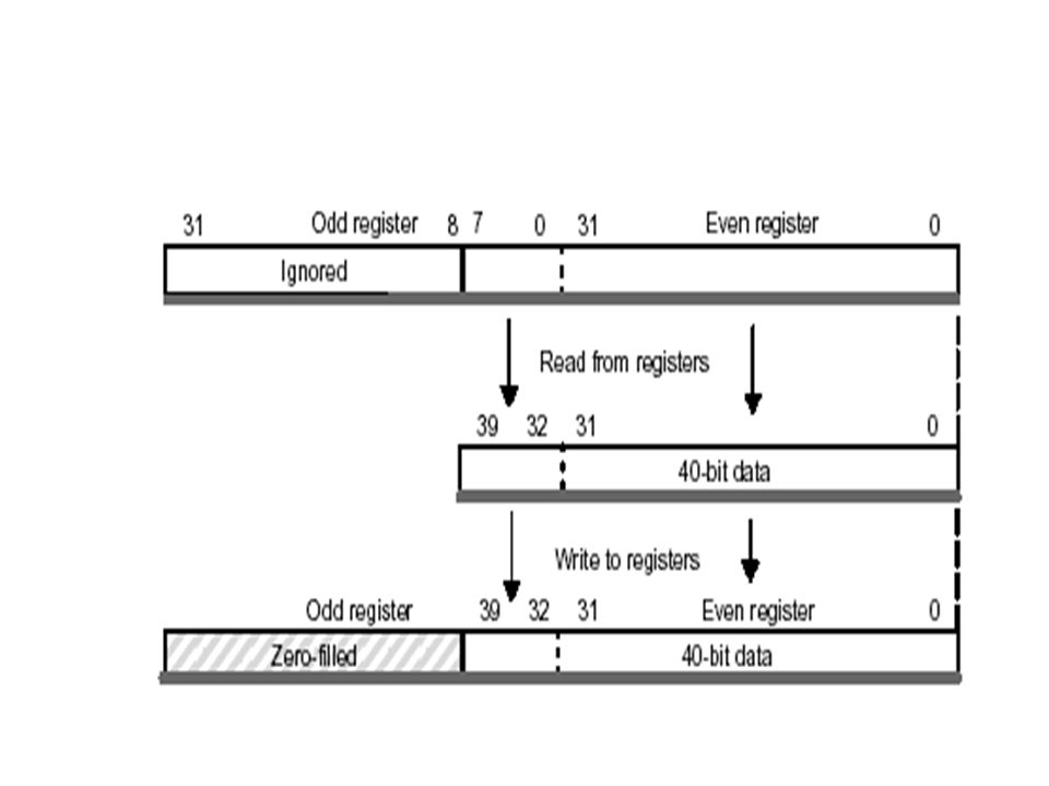
A 40-bit data value can be contained across a register pair. The 32 least significant bits (LSBs) are stored in the even register (e.g.,A2) and the remaining 8 bits are stored in the 8LSBs of the next-upper (odd) register (A3). A similar scheme is used to hold a 64-bit double-precision value within a pair of registers (even and odd).
 are stored in the even register (e.g.,A2) and the remaining 8 bits are stored in the 8LSBs of the next-upper (odd) register (A3). A similar scheme is used to hold a 64-bit double-precision value within a pair of registers (even and odd)..")
45
Addressing modes Determines how one access memory Addressing refers to means to specify location of operands for instructions - types of addressing are called addressing modes - operands may be input operands for the operation as well as results of the operation Addressing modes supported by the TMS320C67x include register-indirect, indexed register-indirect, and modulo addressing (circular addressing). Immediate data is also supported. The TMS320C67x does not support modulo addressing for 64-bit data.

46
ADD.L1 -13,A1,A6 (implied) ADD.L1 A7,A6,A7 not supported LDW.L1 *A5++[8],A1 Immediate – The operand is part of the instruction Register – The operand is specified in a register Direct – The address of the operand is part of the instruction (added to imply memory page) Indirect – The address of the operand is stored in a register
![ADD.L1 -13,A1,A6 (implied) ADD.L1 A7,A6,A7 not supported LDW.L1 *A5++[8],A1 Immediate – The operand is part of the instruction Register – The operand is specified in a register Direct – The address of the operand is part of the instruction (added to imply memory page) Indirect – The address of the operand is stored in a register](http://images.slideplayer.com/11/3251968/slides/slide_46.jpg "ADD.L1 -13,A1,A6 (implied) ADD.L1 A7,A6,A7 not supported LDW.L1 *A5++[8],A1 Immediate – The operand is part of the instruction Register – The operand is specified in a register Direct – The address of the operand is part of the instruction (added to imply memory page) Indirect – The address of the operand is stored in a register")
47
Register-Indirect Addressing Operand is located in memory address stored in a register Special group of registers can be used to store addresses (address registers) Most important addressing mode in DSPs Efficient from instruction set point of view Few bits are needed to indicate address of operand 32 registers(A0-A15,B0-B15) are used as pointers Indirect addressing uses ‘ * ’ in conjunction with one of the 32 registers
 Most important addressing mode in DSPs Efficient from instruction set point of view Few bits are needed to indicate address of operand 32 registers(A0-A15,B0-B15) are used as pointers Indirect addressing uses ‘ * ’ in conjunction with one of the 32 registers")
48
1. * R – register R contains address of a memory location where a data value is stored 2. * R++ (d) - register R contains memory address - after the memory address is used, R is postincremented such that new address is R+1 if d=1 - double minus (- -) update the address by d-1 3. * ++ R(d) - address is preincremented or offset by d - current address is R+d or R-d 4. * + R(d) - address is preincremented by d, such that the current address is R+d - however R pre increments without modification - unlike previous case, R is not updated or modified
 - register R contains memory address - after the memory address is used, R is postincremented such that new address is R+1 if d=1 - double minus (- -) update the address by d-1 3. * ++ R(d) - address is preincremented or offset by d - current address is R+d or R-d 4. * + R(d) - address is preincremented by d, such that the current address is R+d - however R pre increments without modification - unlike previous case, R is not updated or modified.")
49
Delay Line implemented with shifting of sample

50
Delay Line pointer manipulation using Circular Addressing

51
Circular addressing Circular addressing is used to create a circular buffer Buffer is created in hardware and is very useful for applications like digital filtering This addressing mode in conjunction with circular buffer updates samples by shifting data without creating overhead as in direct shifting When pointer reaches bottom location, and when incremented the pointer is automatically wrapped around to the top location. Two independent buffers are available using BK0 and BK1 within the AMR register Registers A4-A7 and B4-B7 in conjunction with.D unit can be used as pointers MVC (move constant) is the only instruction to access AMR and other control registers
 is the only instruction to access AMR and other control registers.")
52
Circular Buffer At the beginning of each sample period, a new sample will be read into the circular buffer,overwriting the oldest sample. The newest sample x(n) will be stored at the memory location pointed at by auxiliary register AR(i).
 will be stored at the memory location pointed at by auxiliary register AR(i)..")
53
The need of processing the digital signals in real time, evolves the concept of Circular Buffering. Circular buffers are used to store the most recent values of a continually updated signal. Circular buffering allows processors to access a block of data sequentially and then automatically wrap around to the beginning address exactly the pattern used to access coefficients in FIR filter. Circular buffering also very helpful in implementing first-in, first-out buffers, commonly used for I/O and for FIR delay lines. Most DSP Implement Circular addressing in hardware in order to conserve memory and minimizing software overhead.

54
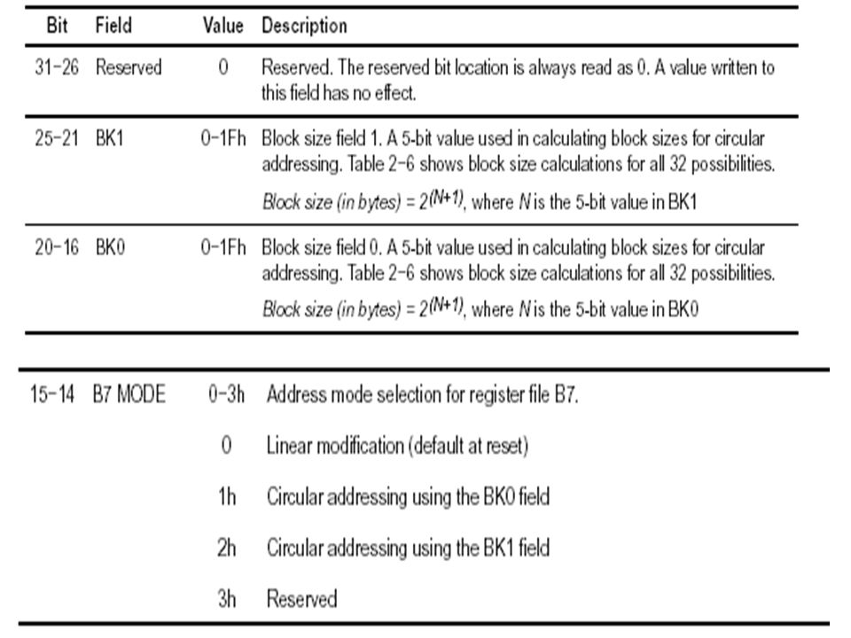
Addressing Mode Register (AMR) For each of the eight registers (A4–A7, B4–B7) that can perform linear or circular addressing, the addressing mode register (AMR) specifies the addressing mode. A 2-bit field for each register selects the address modification mode: linear (the default) or circular mode. With circular addressing, the field also specifies which BK (block size) field to use for a circular buffer. In addition, the buffer must be aligned on a byte boundary equal to the block size.
 or circular mode. With circular addressing, the field also specifies which BK (block size) field to use for a circular buffer. In addition, the buffer must be aligned on a byte boundary equal to the block size..")
55
AMR mode and description Mode description 00 for linear addressing 01 for circular addressing using BK0 For circular addressing using BK1 reserved

60
Block size = 2 N+1 bytes

61
Eg: MVK.S2 0X0004,B2 ; lower 16 bits to B2 MVKLH.S2 0x0005,B2 ; upper 16 bits to B2 The value 0x0004 =(0100) into 16 LSB of AMR sets bit 2 (third bit) to 1 and all other bits to zero. This sets the mode to 01 and selects register A5 as pointer to buffer using BK0 The value 0x0005 =(0101) into 16 MSB of AMR sets bits 16 and 18 to 1. This corresponds to value of N used to select size of buffer = 2 N+1 = 64 bytes using BKO
 into 16 MSB of AMR sets bits 16 and 18 to 1. This corresponds to value of N used to select size of buffer = 2 N+1 = 64 bytes using BKO.")
62
Instruction set They are designed to make maximum use of the processors’ resources and at the same time minimize the memory space required to store the instructions. Minimizing the storage space ensures the cost effectiveness of the overall system. To ensure the maximum use of hardware of the DSP, the instructions are designed to perform several parallel operations in a single instruction, typically including fetching of data in parallel with main arithmetic operation.

63
Assembly Format Label || [ ] Instruction Unit Operands ;comments A label, if present, represents a specific address or memory location that contains an instruction or data. The parallel bars (||) are there if the instruction is being executed in parallel with the previous instruction. The subsequent field is optional to make the associated instruction conditional. Eg: [A2] specifies that the associated instruction executes if A2 is not zero. On the other hand, with [!A2], the associated instruction executes if A2 is zero.
![Assembly Format Label || [ ] Instruction Unit Operands ;comments A label, if present, represents a specific address or memory location that contains an instruction or data.](http://images.slideplayer.com/11/3251968/slides/slide_63.jpg "The parallel bars (||) are there if the instruction is being executed in parallel with the previous instruction. The subsequent field is optional to make the associated instruction conditional. Eg: [A2] specifies that the associated instruction executes if A2 is not zero. On the other hand, with [!A2], the associated instruction executes if A2 is zero..")
64
'C6x Instruction Set (by category) Arithmetic ABS ADD ADDA ADDK ADD2 MPY MPYH NEG SMPY SMPYH SADD SAT SSUB SUB SUBA SUBC SUB2 ZERO Program Ctrl B IDLE NOP Logical AND CMPEQ CMPGT CMPLT NOT OR SHL SHR SSHL XOR Data Mgmt LDB/H/W MV MVC MVK MVKL MVKH MVKLH STB/H/W Bit Mgmt CLR EXT LMBD NORM SET
 Arithmetic ABS ADD ADDA ADDK ADD2 MPY MPYH NEG SMPY SMPYH SADD SAT SSUB SUB SUBA SUBC SUB2 ZERO Program Ctrl B IDLE NOP Logical AND CMPEQ CMPGT CMPLT NOT OR SHL SHR SSHL XOR Data Mgmt LDB/H/W MV MVC MVK MVKL MVKH MVKLH STB/H/W Bit Mgmt CLR EXT LMBD NORM SET")
65
'C6x Instruction Set (by unit).S Unit MVKLH NEG NOT OR SET SHL SHR SSHL SUB SUB2 XOR ZERO ADD ADDK ADD2 AND B CLR EXT MV MVC MVK MVKL MVKH.M Unit SMPY SMPYH MPY MPYH.L Unit NOT OR SADD SAT SSUB SUB SUBC XOR ZERO ABS ADD AND CMPE Q CMPG T CMPLT LMBD MV NEG NORM.D Unit STB/H/W SUB SUBA ZERO ADD ADDA LDB/H/W MV NEG Other IDLENOP
.S Unit MVKLH NEG NOT OR SET SHL SHR SSHL SUB SUB2 XOR ZERO ADD ADDK ADD2 AND B CLR EXT MV MVC MVK MVKL MVKH.M Unit SMPY SMPYH MPY MPYH.L Unit NOT OR SADD SAT SSUB SUB SUBC XOR ZERO ABS ADD AND CMPE Q CMPG T CMPLT LMBD MV NEG NORM.D Unit STB/H/W SUB SUBA ZERO ADD ADDA LDB/H/W MV NEG Other IDLENOP")
66
‘C67x Add’l Instructions (by unit).S Unit CMPLTDP RCPSP RCPDP RSQRSP RSQRDP SPDP ABSSP ABSDP CMPGTSP CMPEQSP CMPLTSP CMPGTDP CMPEQDP.M Unit MPYI MPYID MPYSP MPYDP.L Unit INTSP INTSPU SPINT SPTRUNC SUBSP SUBDP ADDDP ADDSP DPINT DPSP INTDP INTDPU.D Unit ADDADLDDW
.S Unit CMPLTDP RCPSP RCPDP RSQRSP RSQRDP SPDP ABSSP ABSDP CMPGTSP CMPEQSP CMPLTSP CMPGTDP CMPEQDP.M Unit MPYI MPYID MPYSP MPYDP.L Unit INTSP INTSPU SPINT SPTRUNC SUBSP SUBDP ADDDP ADDSP DPINT DPSP INTDP INTDPU.D Unit ADDADLDDW")
67
Add/Subtract/Multiply ADD.L1 A3,A7,A7 ;add A3 + A7 = A7 (accum in A7) adds the values in registers A3 and A7 and places the result in register A7. The unit.L1 is optional. If the destination or result is in B7, the unit would be.L2. SUB.S1 A1,1,A1 ;subtract 1 from A1

68
MPY.M2 A7,B7,B6 ;multiply 16 LSBs of A7,B7 => B6 || MPYH.M1 A7,B7,A6 ;multiply 16MSBs of A7,B7 =>A6 multiplies the lower or least significant 16 bits (LSBs) of both A7 and B7 and places the product in B6, in parallel with a second instruction that multiplies the higher or most significant 16 bits (MSBs) of A7 and B7 and places the result in A6.
 of both A7 and B7 and places the product in B6, in parallel with a second instruction that multiplies the higher or most significant 16 bits (MSBs) of A7 and B7 and places the result in A6.")
69
Load/Store LDH.D2 *B2++,B7 ;load (B2) =>B7, increment B2 || LDH.D1 *A2++,A7 ;load (A2) -> A7, increment A2 The instruction LDW loads a 32-bit word. Two paths using D1 and.D2 allow for the loading of data from memory to registers A and B using the instruction LDW. The double-word load floating-point instruction LDDW on the C6711 can simultaneously load two 32-bit registers into side A and two 32-bit registers into side B.

70
Store STW.D1 A1,*+A4[20] ;store A1->(A4) offset by 20 The address register A4 is preincremented - with offset, but it is not modified (two plus signs are used if A4 is to be modified).
![Store STW.D1 A1,*+A4[20] ;store A1->(A4) offset by 20 The address register A4 is preincremented - with offset, but it is not modified (two plus signs are used if A4 is to be modified).](http://images.slideplayer.com/11/3251968/slides/slide_70.jpg "Store STW.D1 A1,*+A4[20] ;store A1->(A4) offset by 20 The address register A4 is preincremented - with offset, but it is not modified (two plus signs are used if A4 is to be modified).")
71
Branch

72
Assembler Directive An assembler directive is a message for the assembler and is not an instruction. It is resolved during the assembling process and does not occupy memory space as an instruction does. It does not produce executable code.

73
1).short: to initialize a 16-bit integer. 2).int: to initialize a 32-bit integer (also.word or.long). 3).float: to initialize a 32-bit IEEE single- precision constant. 4).double: to initialize a 64-bit IEEE double- precision constant.
.int: to initialize a 32-bit integer (also.word or.long). 3).float: to initialize a 32-bit IEEE single- precision constant. 4).double: to initialize a 64-bit IEEE double- precision constant..")
74
ASM STATEMENT WITHIN C Assembly instructions and directives can be incorporated within a C program using the asm statement. The syntax is asm (“assembly code”); The assembly line of code within the set of quotes has the same format as a valid assembly statement. If the instruction has a label, the first character of the label must start after the first quote so that it is in column 1. The assembly statement should be valid since the compiler does not check it for syntax error but copies it directly into the compiled output file. If the assembly statement has a syntax error, the assembler would detect it.
; The assembly line of code within the set of quotes has the same format as a valid assembly statement. If the instruction has a label, the first character of the label must start after the first quote so that it is in column 1. The assembly statement should be valid since the compiler does not check it for syntax error but copies it directly into the compiled output file. If the assembly statement has a syntax error, the assembler would detect it..")
75
C-CALLABLE ASSEMBLY FUNCTION Register B3 is preserved and is used to contain the return address of the calling function. An external declaration of an assembly function called within a C program using extern is optional. For example, extern int func(); is optional with the assembly function func returning an integer value.
; is optional with the assembly function func returning an integer value..")
76
Timer Two 32-bit timers can be used to time and count events or to interrupt the CPU. A timer can direct an external ADC to start conversion or the DMA controller to start a data transfer. Registers – Time period register, - specifies the timer’s frequency – Timer counter register, - contains the value of the incrementing counter; – Timer control register, - monitors the timer’s status.

77
Timer The ’C67x has two 32-bit general-purpose timers that can be used to: – Time events – Count events – Generate pulses – Interrupt the CPU – Send synchronization events to the DMA controller

79
The timer works in one of the two signaling modes depending on whether clocked by an internal or an external source. The timer has an input pin (TINP) and an output pin (TOUT). The TINP pin can be used as a general purpose input, and the TOUT pin can be used as a general-purpose output. When an internal clock is provided, the timer generates timing sequences to trigger peripheral or external devices such as DMA controller or A/D converter respectively. When an external clock is provided, the timer can count external events and interrupt the CPU after a specified number of events.
 and an output pin (TOUT). The TINP pin can be used as a general purpose input, and the TOUT pin can be used as a general-purpose output. When an internal clock is provided, the timer generates timing sequences to trigger peripheral or external devices such as DMA controller or A/D converter respectively. When an external clock is provided, the timer can count external events and interrupt the CPU after a specified number of events..")
80
Interrupts The C6711device supports 16 prioritized interrupts Types of interrupts: Reset Maskable Non maskable

81
Interrupt process An interrupt can be issued internally or externally. An interrupt stops the current CPU process so that it can perform a required task initiated by the interrupt. The program flow is redirected to an interrupt service routine (ISR). The conditions of the current process must be saved so that they can be restored after the interrupt task is performed. On interrupt, registers are saved and processing continues to an ISR. Then the registers are restored.
. The conditions of the current process must be saved so that they can be restored after the interrupt task is performed. On interrupt, registers are saved and processing continues to an ISR. Then the registers are restored..")
82
Reset (RESET) Reset is the highest priority interrupt and is used to halt the CPU and return it to a known state. The reset interrupt is unique in a number of ways: - RESET is an active-low signal. All other interrupts are active-high signals. - RESET must be held low for 10 clock cycles before it goes high again to reinitialize the CPU properly. - The instruction execution in progress is aborted and all registers are returned to their default states. -

83
Nonmaskable Interrupt (NMI) - NMI is the second-highest priority interrupt - generally used to alert the CPU of a serious hardware problem such as imminent power failure. - For NMI processing to occur, the non maskable interrupt enable (NMIE) bit in the interrupt enable register must be set to 1.
 bit in the interrupt enable register must be set to 1..")
84
Maskable interrupt process 1. The GIE bit is set to 1. 2. The NMIE bit is set to 1. 3. The appropriate IE bit is set to 1. 4. The corresponding IFR bit is set to 1.

86
Maskable Interrupts (INT4−INT15) - These have lower priority than the NMI and reset interrupts. - These interrupts can be associated with external devices, on-chip peripherals, software control etc. The interrupt source for interrupts 4-15 can be programmed by modifying the selector value (binary value) in the corresponding fields of the Interrupt
 in the corresponding fields of the Interrupt.")
87
CSR (control status register): contains the global interrupt enable (GIE) bit and other control/status bits IER (interrupt enable register): enables/disables individual interrupts IFR (interrupt flag register): displays status of interrupts ISR (interrupt set register): sets pending interrupts ICR (interrupt clear register): clears pending interrupts ISTP (interrupt service table pointer): locates an ISR IRP (interrupt return pointer) NRP (nonmaskable interrupt return pointer)
: contains the global interrupt enable (GIE) bit and other control/status bits IER (interrupt enable register): enables/disables individual interrupts IFR (interrupt flag register): displays status of interrupts ISR (interrupt set register): sets pending interrupts ICR (interrupt clear register): clears pending interrupts ISTP (interrupt service table pointer): locates an ISR IRP (interrupt return pointer) NRP (nonmaskable interrupt return pointer)")
88
Interrupt Acknowledgment The signals IACK and INUMx (INUM0 through INUM3) are pins on the C6x that acknowledge an interrupt has occurred and is being processed. The four INUMx signals indicate the number of the interrupt being processed. INUM3 = 1 (MSB), INUM2 = 0, INUM1 = 1, INUM0 = 1 (LSB) corresponds to (1011)b = 11, indicating that INT11 is being processed. The IE11 bit is set to 1 to enable INT11. The interrupt flag register (IFR) can be read to verify that bit IF11 is set to 1. Writing a 1 to a bit in the interrupt set register (ISR) causes the corresponding interrupt flag to be set in IFR; whereas a 1 to a bit in the interrupt clear register (ICR) causes the corresponding interrupt to be cleared.
, INUM2 = 0, INUM1 = 1, INUM0 = 1 (LSB) corresponds to (1011)b = 11, indicating that INT11 is being processed. The IE11 bit is set to 1 to enable INT11. The interrupt flag register (IFR) can be read to verify that bit IF11 is set to 1. Writing a 1 to a bit in the interrupt set register (ISR) causes the corresponding interrupt flag to be set in IFR; whereas a 1 to a bit in the interrupt clear register (ICR) causes the corresponding interrupt to be cleared..")
89
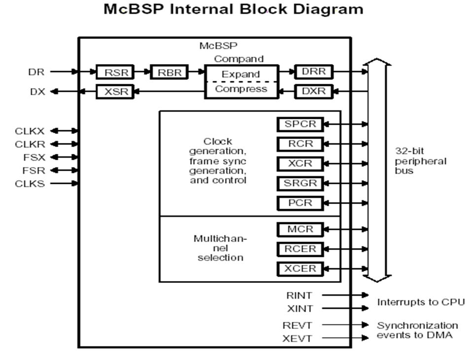
Multichannel Buffered Serial Port (McBSP) The standard serial port interface provides: – Full-duplex communication – Double-buffered data registers, which allow a continuous data stream – Independent framing and clocking for reception and transmission – Direct interface to industry-standard codecs, analog interface chips (AICs), and other serially connected A/D and D/A devices - Multi channel transmission and reception of up to 128 channels. – An element sizes of 8, 12, 16, 20, 24, or 32-bit. - 8-bit data transfers with LSB or MSB first.

91
The McBSP consists of a data path and a control path that connect to external devices. Separate pins for transmission and reception communicate data to these external devices. Four other pins communicate control information (clocking and frame synchronization). The device communicates to the McBSP using 32-bit-wide control and data registers accessible via the internal peripheral bus. Pin Description CLKR Receive clock CLKX Transmit clock CLKS External clock DR Received serial data DX Transmitted serial data FSR Receive frame synchronization FSX Transmit frame synchronization
. The device communicates to the McBSP using 32-bit-wide control and data registers accessible via the internal peripheral bus. Pin Description CLKR Receive clock CLKX Transmit clock CLKS External clock DR Received serial data DX Transmitted serial data FSR Receive frame synchronization FSX Transmit frame synchronization.")
92
CPU or DMA write the DATA to be transmitted to the Data transmit register (DXR) which is shifted out to DX via the transmit shift register (XSR). Similarly, receive data on the DR pin is shifted into the receive shift register (RSR) and copied into the receive buffer register (RBR). RBR is then copied to DRR, which can be read by the CPU or the DMA controller. This allows internal data movement and external data communications simultaneously. The following control registers are used in multichannel operation: The multi channel control register (MCR) The transmit channel enable register (XCER) The receive channel enable register (RCER)
 and copied into the receive buffer register (RBR). RBR is then copied to DRR, which can be read by the CPU or the DMA controller. This allows internal data movement and external data communications simultaneously. The following control registers are used in multichannel operation: The multi channel control register (MCR) The transmit channel enable register (XCER) The receive channel enable register (RCER).")
93
Other registers for clock generation, frame synchronization and control are: serial port control register (SPCR) receive control register (RCR) transmit control register (XCR) pin control register (PCR) Sample rate generator register (SRGR)
 receive control register (RCR) transmit control register (XCR) pin control register (PCR) Sample rate generator register (SRGR)")
94
DMA Direct Memory Access transfers data to or from the processor’s memory without the involvement of the processor itself. DMA is commonly used to provide improved performance with input/output devices. Rather than have the processor read data from an I/O device and copy the data into memory or vice versa, a separate DMA controller can handle such transfers in parallel. The processor loads the DMA controller with control information including the starting address for the transfer, the number of words to be transferred, the source and the destination.

95
The DMA controller uses the bus request pin to notify the DSP core that it is ready to make a transfer to or from external memory. The DSP core completes its current instruction, releases control of external memory and signals the DMA controller via the bus grant pin that the DMA transfer can proceed. The DMA controller then transfers the specified number of data words and optionally signals completion through an interrupt. Some processor can also have multiple channels DMA managing DMA transfers in parallel.

96
Data Allocation Blocks of code and data can be allocated in memory within sections specified in the linker command file. These sections can be either initialized or uninitialized. Initialized or uninitialized sections, except.text, cannot be allocated into internal program memory.

97
The initialized sections are: 1..cinit: for global and static variables 2..const: for global and static constant variables 3..switch: contains jump tables for large switch statements 4..text: for executable code and constants The uninitialized sections are: 1..bss: for global and static variables 2..far: for global and static variables declared far 3..stack: allocates memory for the system stack 4..sysmem: reserves space for dynamic memory allocation used by the malloc, calloc, and realloc functions

98
Data Alignment The C6x always accesses aligned data which allows it to address bytes, half-words, and words (32 bits)
")
99
Control Register File

100
Addressing mode register (AMR) - specifies the addressing mode Control status register (CSR) - contains control and status bits. Interrupt clear register (ICR) - allows you to manually clear the maskable interrupts (INT15- INT4) in the interrupt flag register (IFR). - Writing a 1 to any of the bits in ICR causes the corresponding interrupt flag (IFn) to be cleared in IFR. - Writing a 0 to any bit in ICR has no effect. - You cannot set any bit in ICR to affect NMI or reset. Interrupt enable register (IER) - enables and disables individual interrupts.
 - allows you to manually clear the maskable interrupts (INT15- INT4) in the interrupt flag register (IFR). - Writing a 1 to any of the bits in ICR causes the corresponding interrupt flag (IFn) to be cleared in IFR. - Writing a 0 to any bit in ICR has no effect. - You cannot set any bit in ICR to affect NMI or reset. Interrupt enable register (IER) - enables and disables individual interrupts..")
101
The interrupt flag register (IFR) - contains the status of INT4-INT15 and NMI interrupt. - Each corresponding bit in the IFR is set to 1 when that interrupt occurs; otherwise, the bits are cleared to 0. - If you want to check the status of interrupts, use the MVC instruction to read the IFR. The interrupt return pointer register (IRP) - contains the return pointer that directs the CPU to the proper location to continue program execution after processing a maskable interrupt. - A branch using the address in IRP (B IRP) in your interrupt service routine returns to the program flow when interrupt servicing is complete.
 - contains the return pointer that directs the CPU to the proper location to continue program execution after processing a maskable interrupt. - A branch using the address in IRP (B IRP) in your interrupt service routine returns to the program flow when interrupt servicing is complete..")
102
The interrupt set register (ISR) - allows you to manually set the maskable interrupts (INT15- INT4) in the interrupt flag register (IFR). - Writing a 1 to any of the its in ISR causes the corresponding interrupt flag (IFn) to be set in IFR. - Writing a 0 to any bit in ISR has no effect. - You cannot set any bit in ISR to affect NMI or reset. The interrupt service table pointer register (ISTP) - is used to locate the interrupt service routine (ISR). The NMI return pointer register (NRP) - contains the return pointer that directs the CPU to the proper location to continue program execution after NMI processing. - A branch using the address in NRP (B NRP) in your interrupt service routine returns to the program flow when NMI servicing is complete. The E1 phase program counter (PCE1) - contains the 32-bit address of the fetch packet in the E1 pipeline phase.
 to be set in IFR. - Writing a 0 to any bit in ISR has no effect. - You cannot set any bit in ISR to affect NMI or reset. The interrupt service table pointer register (ISTP) - is used to locate the interrupt service routine (ISR). The NMI return pointer register (NRP) - contains the return pointer that directs the CPU to the proper location to continue program execution after NMI processing. - A branch using the address in NRP (B NRP) in your interrupt service routine returns to the program flow when NMI servicing is complete. The E1 phase program counter (PCE1) - contains the 32-bit address of the fetch packet in the E1 pipeline phase..")
Similar presentations


 Dr. Konstantinos Tatas.>")


 is used in a wide variety of applications, and it is hard to find a good.>")

