Download presentation
Presentation is loading. Please wait.

1
Equipe Couches Nanométriques : Formation, Interfaces, Défauts
SAFIR : Un accélérateur Van de Graaff pour l’analyse de couches minces et ultra-minces Equipe Couches Nanométriques : Formation, Interfaces, Défauts SAFIR

4
General purpose IBA chambers UHV goniometer chamber
The SAFIR Laboratory General purpose IBA chambers 10-7 mbar RBS, NRA, NRP, ERDA Fast opening and pumping Large sample holder Goniometer chamber for channeling UHV goniometer chamber 10-11 mbar LEED/Auger Channeling/Blocking Evaoprators Sample heating and cooling Rare gas handling 2.5 MV Van de Graaff 1H, 2H, 3He, 4He, C,N,O etc Stable operation down to < 150keV Beam energy resolution eV Several mA in 2mm at target MEIS ~10 permanent research/teaching staff 3 1/3 dedicated technical staff

5
Ion Beam Analysis (IBA)
Energy loss PIXE Elastic Scattering Nuclear Reactions Narrow resonance profiling Energy range MeV Projectiles protons, deuterons, alphas, 3He

6
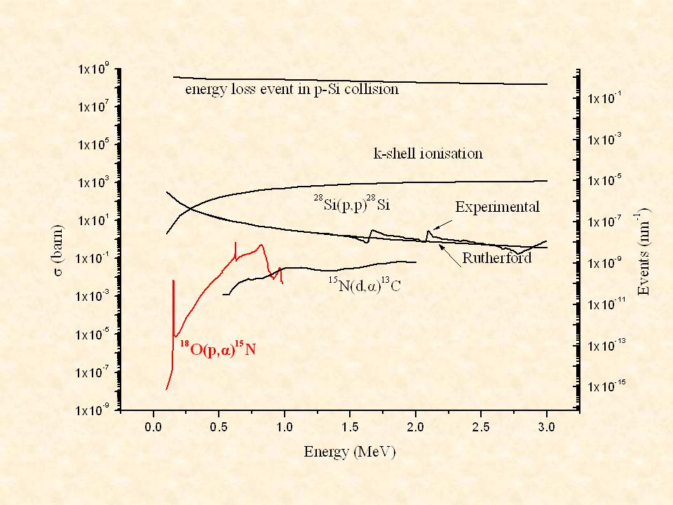
Quelques sections efficaces
Pour un proton dans le silicium

7
The stopping power

8
The stopping power E-DE E Dx N atoms cm-3 Density r g cm-3
Units : eV cm2 atom-1 eV cm2 mg-1 eV nm-1

9
Rutherford Backscattering Spectrometry RBS

10
Détecteur particules 4He+ Bague isolante Porte échantillon

12
E Nombre de coups x x x E K2E0 K1E0 Atome d’Aluminium Atome d’Or
Détecteur particules

13
RBS - principle E1 = k1 E E2 = k2 E 4He+ Energy E Detector Yield
Energy gives mass scale Energy loss gives depth scale Intensity gives concentration Analytique ! Beam loses energy 4He+ Energy E Trace of heavy element in a light substrate - eg Au in Si Si Depth Si surface Detector Au Depth Yield Au surface E E2 Energy

14
Real RBS - Cu/Al2O3 Taken from work with R. Serna et al, Instituto de Optica, Madrid Composite formed by alternate pulsed laser deposition of Cu and Al2O3. Non-linear optical properties – amplification … Structure supposed for RBS simulation Surfaces layers, plus 7 times 90x1015 cm-2 Al2O (10nm) 45 Al2O3+30%Cu plus 120x1015 cm-2 Al2O3 32 Al2O3+70%Cu Artificially nanostructured Cu: Al2O3 films produced by pulsed laser ablation. R. Serna, C.N. Afonso, C. Ricolleau, Y. Wang, Y. Zheng, M. Gandais, I. Vickridge. Appl. Phys. A. 71 (2000),
 45 Al2O3+30%Cu. plus. 120x1015 cm-2 Al2O3. 32 Al2O3+70%Cu. Artificially nanostructured Cu: Al2O3 films produced by pulsed laser ablation. R. Serna, C.N. Afonso, C. Ricolleau, Y. Wang, Y. Zheng, M. Gandais, I. Vickridge. Appl. Phys. A. 71 (2000),")
15
RBS – Anodisation of Au/Al alloy
Au/Al alloy (4.5%Au) Anodic oxide From P. Skeldon et al, Corrosion Centre, University of Manchester H. Habazaki, K. Shimizu, P. Skeldon, G.E. Thompson, G.C. Wood, and X. Zhou, J. Phys. D: Appl. Phys. 30, 1833 (1997).
 Anodic. oxide. From P. Skeldon et al, Corrosion Centre, University of Manchester. H. Habazaki, K. Shimizu, P. Skeldon, G.E. Thompson, G.C. Wood, and X. Zhou, J. Phys. D: Appl. Phys. 30, 1833 (1997).")
16
(conditions favorables)
RBS : Performances (conditions favorables) Sensibilité : at/cm2 Résolution en profondeur : 10 nm Résolution en masse : 1 amu jusqu'à ~40 amu Durée d'analyse : 5 minutes Nécessite vide : <10-5 mbar
 Sensibilité : 1014 at/cm2. Résolution en profondeur : 10 nm. Résolution en masse : 1 amu jusqu à ~40 amu. Durée d analyse : 5 minutes. Nécessite vide : <10-5 mbar.")
17
Nuclear Reactions

18
Nuclear Reactions Reaction Q (MeV) 12C(d,p0)13C 2.72 12C(d,p1)13C
Charged particle induced reactions : NRA Nuclear Reaction Analysis Interaction is inelastic : internal energy needs to be included in the kinematics. NRA is isotope-sensitive (residual nucleus in ground state) (residual nucleus in nth excited state, of energy En) Reaction Q (MeV) 12C(d,p0)13C 2.72 12C(d,p1)13C -0.34 16O(d,p0)17O 1.92 16O(d,p1)17O 1.05
 (residual nucleus in nth excited state, of energy En) Reaction. Q (MeV) 12C(d,p0)13C C(d,p1)13C O(d,p0)17O O(d,p1)17O")
19
NRA Kinematics E.g. (d,p) reactions on light nuclei
qlab=150°, Ed=1.4 MeV, mylar foil 12mm stops 0.9 MeV 2H 2.8 MeV 4He

20
NRA Cross sections Strong variation with E0 Strong variation with q
Few reliable nuclear models see SigmaCalc See and R33 files distributed with SimNRA

21
NRA Thin Sample Principle
Cross section 2H+ 12 16O(d,p1)17O qlab=150° Absorber foil 10 8 ) -1 Detector (mb sr 16O(d,p1)17O 6 s 4 16O(d,p0)17O 2 400 500 600 700 800 900 1000 1100 1200 Energy (keV) Yield 12C(d,p0)13O Incident beam energy Energy (MeV)
17O. qlab=150° Absorber foil ) -1. Detector. (mb sr. 16O(d,p1)17O. 6. s O(d,p0)17O Energy (keV) Yield. 12C(d,p0)13O. Incident beam energy. Energy (MeV)")
22
Thin and Thick target NRA spectra
NRA Spectra from thin and thick Ta2O5 with small carbon contamination

23
NRA – isotopic profiling
Simultaneous profiling of 14N and 15N via 14N(d,a1)12C and 14N(d,a0)13C respectively. Nitridation of a Ti6Al4V alloy : artificial hip, to improve biocompatibilty Strong nitrogen exchange between the gas and the nitride is observed. From I.C. Vickridge et al. Nucl. Instr. And Meth. B99 (1995) 454.
12C and 14N(d,a0)13C respectively. Nitridation of a Ti6Al4V alloy : artificial hip, to improve biocompatibilty. Strong nitrogen exchange between the gas and the nitride is observed. From I.C. Vickridge et al. Nucl. Instr. And Meth. B99 (1995) 454.")
24
(conditions favorables)
NRA : Performances (conditions favorables) Sensibilité : at/cm2, 0.1% Résolution en profondeur : 100 nm Spécificité isotopique : Elements légers (H-Si) Durée d'analyse : 5 minutes Nécessite vide : <10-5 mbar
 Sensibilité : 1014 at/cm2, 0.1% Résolution en profondeur : 100 nm. Spécificité isotopique : Elements légers (H-Si) Durée d analyse : 5 minutes. Nécessite vide : <10-5 mbar.")
25
High depth resolution IBA
2MeV 4He in Ni Dx=16nm 500 keV 4He in Si Dx=29nm e.g. RBS, DEdet= 10keV : Reduce Dx? Remove the detector Nuclear Resonance Profiling NRP Reduce DEdet Electrostatic or Magnetic spectrometers MEIS

27
Narrow Resonance Profiling
18O(p,a)15N resonance at 151 keV. 16O2 then 18O2 Si exchange growth SiO2 150 155 160 165 170 175 180 200 400 600 800
15N resonance at 151 keV. 16O2. then. 18O2. Si. exchange. growth. SiO")
28
Growth of SiC nanocrystals at the SiO2/SiC interface
Silicon with thermally grown SiO2 1100°C annealing under CO Quartz furnace 13C180 SiO2 The use of 13C18O allows us to : observe the fate of C only from CO (13C) without being concerned with C contamination quantitatively determine the fate of 18O from the CO (Si16O2 matrix) SiC SiO2 Moiré pattern Si Si Epitaxial 3C - SiC Cross sectional TEM image of a (100) Si/SiO2 system annealed in 100% CO at 1 Bar at 1100oC for 2hrs
 without being concerned with C contamination. quantitatively determine the fate of 18O from the CO (Si16O2 matrix) SiC. SiO2. Moiré pattern. Si. Si. Epitaxial 3C - SiC. Cross sectional TEM image of a (100) Si/SiO2 system annealed in 100% CO at 1 Bar at 1100oC for 2hrs.")
29
Typical excitation curve
18O Excitation curves after 1100°C treatment for 90 min at 350mbar The three regions in the 18O concentration profile reflect 3 processes CO diffusion with exchange in volume Process I Oxygen exchange at surface Process II + oxygen network diffusion Oxygen incorporation at interface Process III Volume 16O-18O exchange Process I Interface reaction CO interstitiel diffusion SiC Process II SiO2 Si An 18O study of the interaction between carbon monoxide and dry thermal SiO2 at 1100°C. Catherine Deville Cavellin, Isabelle Trimaille, Jean-Jacques Ganem, Marie D’Angelo, Ian Vickridge, Anita Pongracz and Gabor Battistig. Journal of Applied Physics (2009), 105, Isotopic tracing study of the growth of silicon carbide nano-crystals at the SiO2/Si interface by CO annealing. A. Pongracz, Y. Hoshino, M. D’Angelo, C. Deville Cavellin, J.-J. Ganem, I. Trimaille, G. Battistig, K.V. Josepovits, I. Vickridge. Journal of Applied Physics (2009) 106,
, 105, Isotopic tracing study of the growth of silicon carbide nano-crystals at the SiO2/Si interface by CO annealing. A. Pongracz, Y. Hoshino, M. D’Angelo, C. Deville Cavellin, J.-J. Ganem, I. Trimaille, G. Battistig, K.V. Josepovits, I. Vickridge. Journal of Applied Physics (2009) 106,")
30
Ratio of O to C incorporated in the interface region
90 min, 1100°C We can now confidently conclude that for each C atom incorporated in a SiC nano-crystal, an oxygen atom is incorprated in the SiO2/Si interfacial region.

31
Medium Energy Ion Scattering
Electrostatic detector Semiconductor detector p-type silicon depleted region undepleted region deposited energy

32
Détecteur électrostatique toroïdal
permettant une analyse simultanée en énergie (profil de composition) en angle (structure) des ions rétro-diffusés dans les premiers nm. Si(100) 13A SiO2 46A La2Si2O7
 en angle (structure) des ions rétro-diffusés dans les premiers nm. Si(100) 13A. SiO2. 46A. La2Si2O7.")
33
MEIS : Typical example Medium Energy Ion Scattering
La2O3 (high k) deposited on Si, then oxidised : chemical reaction … RBS relatively classical 200keV 4He+ dét. 15keV Medium Energy Ion Scattering (from M. Copel et al, IBM Almaden)
 deposited on Si, then oxidised : chemical reaction … RBS relatively classical. 200keV 4He+ dét. 15keV. Medium Energy Ion Scattering. (from M. Copel et al, IBM Almaden)")
34
Comparaison MEIS – RBS RBS MEIS Résolution en profondeur 10 nm 0.3 nm
Profondeur explorable 1mm 20 nm Sensibilité (at.cm-2) 1014 qqs 1012 MAIS : temps d’acquisition des spectres (RBS = 101 minutes, MEIS = 102 minutes dégâts induits dans l’échantillon physique sous-jacente +compliquée, moins bien maitrisée
 qqs MAIS : temps d’acquisition des spectres (RBS = 101 minutes, MEIS = 102 minutes. dégâts induits dans l’échantillon. physique sous-jacente +compliquée, moins bien maitrisée.")
36
One important topic we have not talked about : ion channelling
Amorphisation of Si by implantation of 29Si But, damage …

37
Augmenter l'angle solide des détecteurs de particules, sans perdre en résolution en énergie
Réduire dose nécessaire pour obtenir spectres utiles (Aussi polymères, hydrogène …)
")
38
Design and build large area segmented particle detectors.
Matrice de 16 détecteurs pour ERDA (détection H) Matrice de 16 détecteurs pour RBS 16 spectra collected simultaneously, at various angles 20 to 40 times greater solid angle for detection Spectroscopic tests underway in Rossendorf. Installation at INSP at end 2010 probably… Détecteurs pour tests
 Matrice de 16 détecteurs pour RBS. 16 spectra collected simultaneously, at various angles. 20 to 40 times greater solid angle for detection. Spectroscopic tests underway in Rossendorf. Installation at INSP at end 2010 probably… Détecteurs pour tests.")
Similar presentations


 27 Si Reaction at DRAGON Heather Crawford Simon Fraser University TRIUMF Student Symposium July 27, 2005.>")

.>")
 am Deutschen Elektronen.>")
 Belgium: 1IKS KU Leuven Czech Republic: 2Nucl. Phys. Inst. Acad.>")
 6 Li measurement -Status of.>")


