Download presentation
Presentation is loading. Please wait.

1
Introduction to CCDs Claudio Cumani for ITMNR-5
Optical Detector Team - European Southern Observatory for ITMNR-5 Fifth International Topical Meeting on Neutron Radiography Technische Universität München, Garching, July 26, 2004

2
CCDs - Introduction Charge Coupled Devices (CCDs) were invented in October 19, 1969, by William S. Boyle and George E. Smith at Bell Telephone Laboratories (“A new semiconductor device concept has been devised which shows promise of having wide application”, article on Bell System Technical Journal, 49, (April 1970). CCDs are electronic devices, which work by converting light into electronic charge in a silicon chip (integrated circuit). This charge is digitised and stored as an image file on a computer.
 were invented in October 19, 1969, by William S. Boyle and George E. Smith at Bell Telephone Laboratories. ( A new semiconductor device concept has been devised which shows promise of having wide application , article on Bell System Technical Journal, 49, (April 1970). CCDs are electronic devices, which work by converting light into electronic charge in a silicon chip (integrated circuit). This charge is digitised and stored as an image file on a computer.")
3
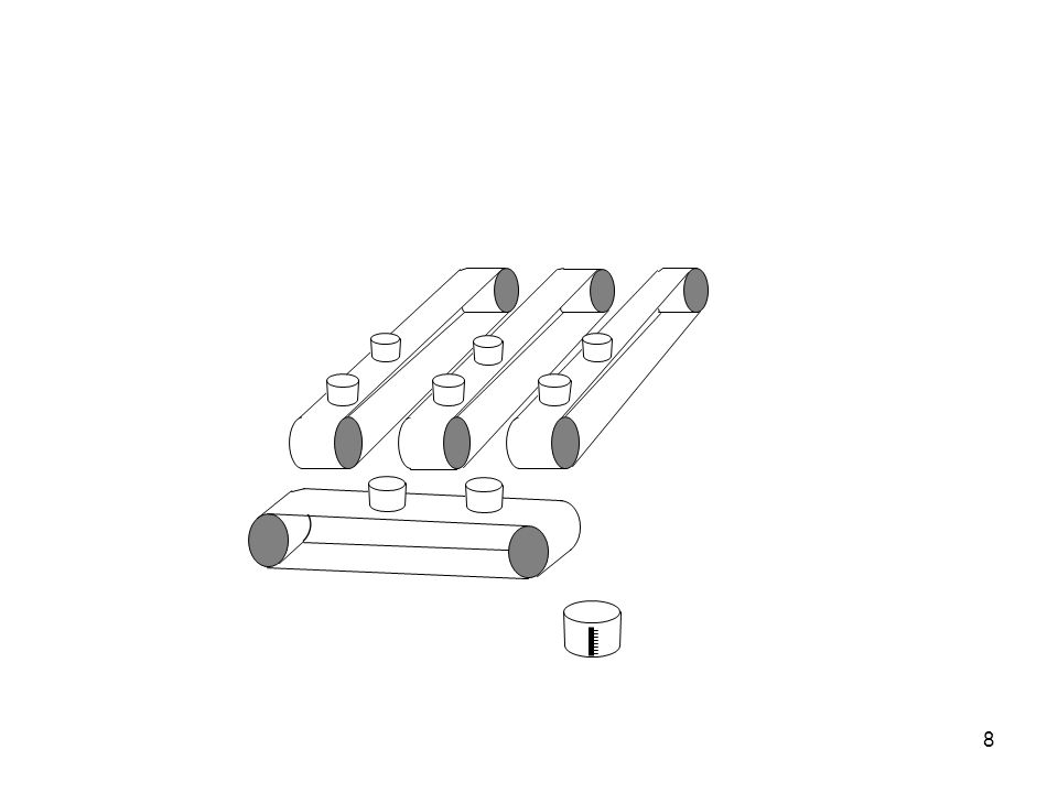
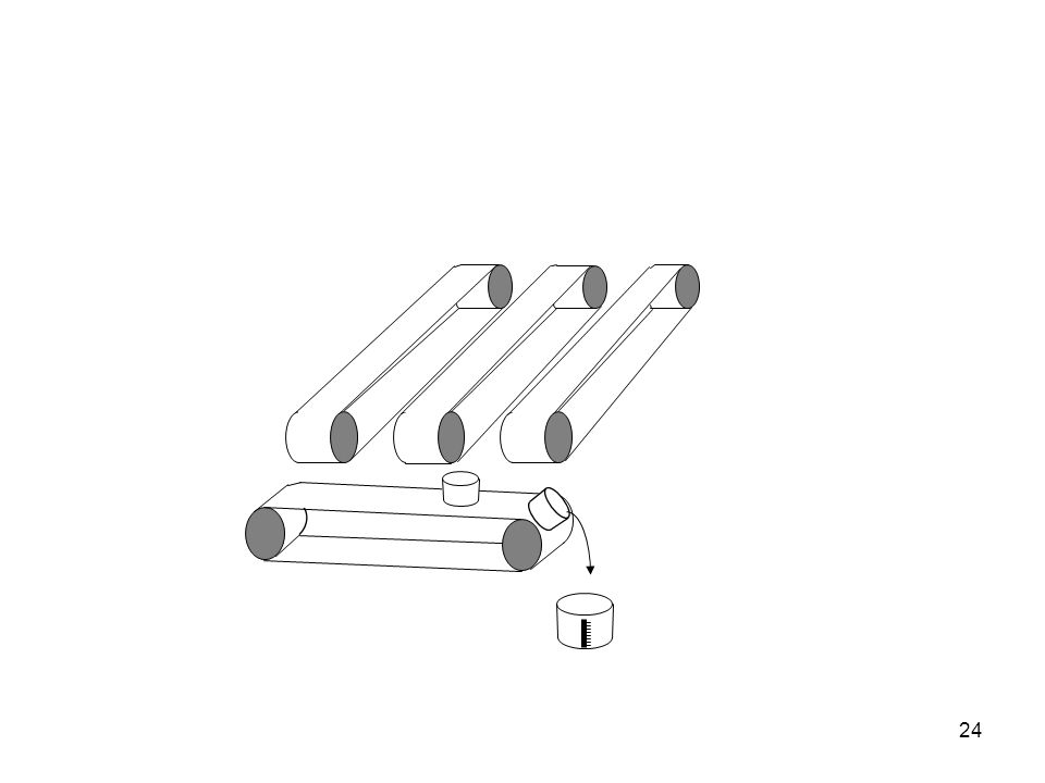
“Bucket brigade” analogy
VERTICAL CONVEYOR BELTS (CCD COLUMNS) RAIN (PHOTONS) BUCKETS (PIXELS) METERING STATION (OUTPUT AMPLIFIER) HORIZONTAL CONVEYOR BELT (SERIAL REGISTER)
 RAIN (PHOTONS) BUCKETS (PIXELS) METERING. STATION. (OUTPUT. AMPLIFIER) HORIZONTAL. CONVEYOR BELT. (SERIAL REGISTER)")
4
Exposure finished, buckets now contain samples of rain.

5
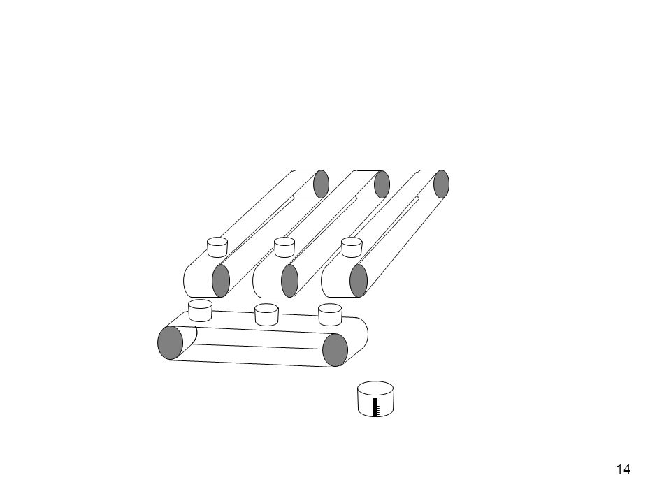
Conveyor belt starts turning and transfers buckets.
Rain collected on the vertical conveyor is tipped into buckets on the horizontal conveyor.

6
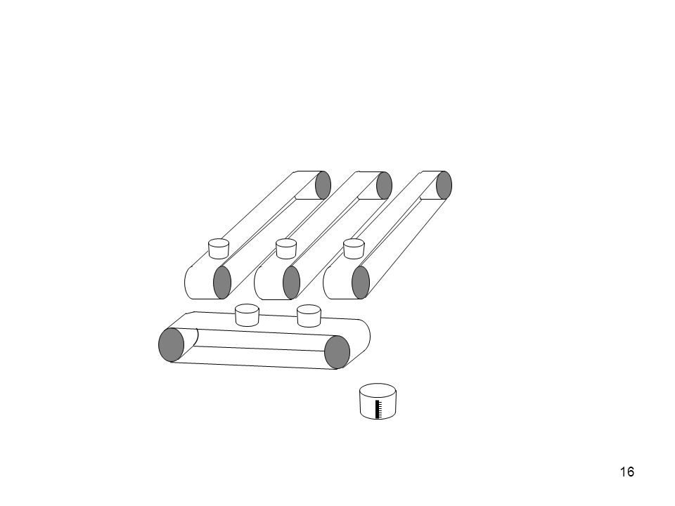
Vertical conveyor stops.
Horizontal conveyor starts up and tips each bucket in turn into the metering station.

7
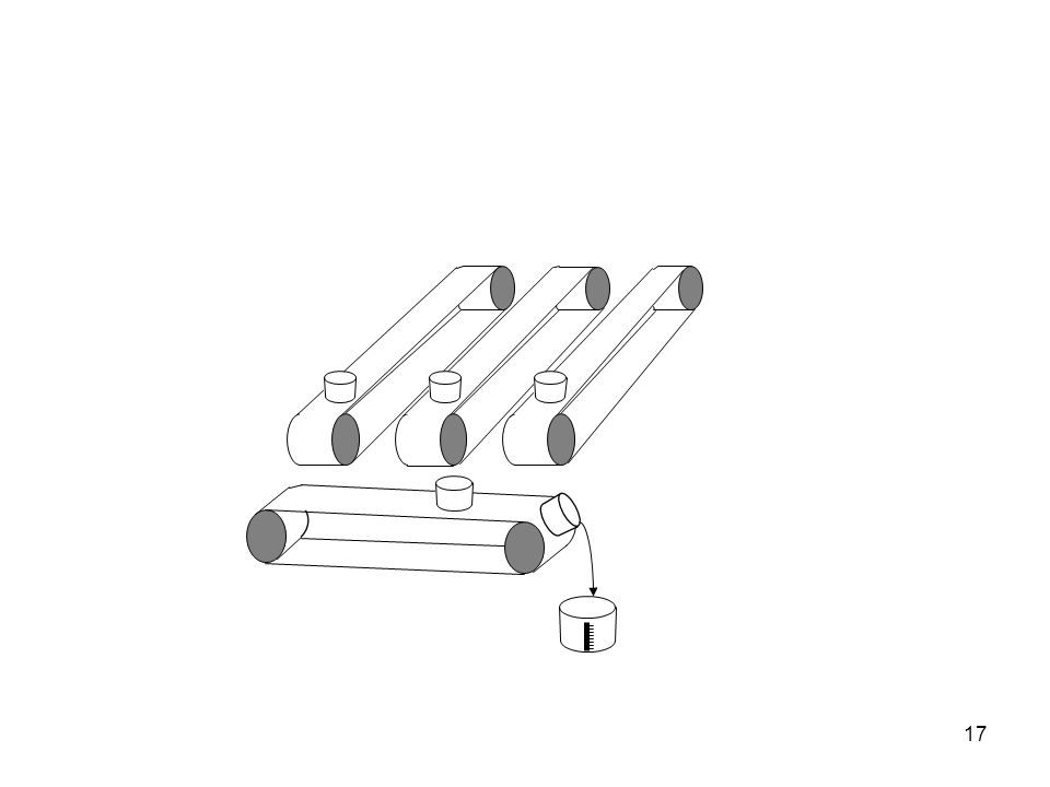
After each bucket has been measured, the metering station is emptied, ready for the next bucket load. `

13
A new set of empty buckets is set up on the horizontal conveyor and the process is repeated.

27
CCD structure A CCD is a two-dimensional array of metal-oxide-semiconductor (MOS) capacitors The charges are stored in the depletion region of the MOS capacitors Charges are moved in the CCD circuit by manipulating the voltages on the gates of the capacitors so as to allow the charge to spill from one capacitor to the next (thus the name “charge-coupled” device) A charge detection amplifier detects the presence of the charge packet, providing an output voltage that can be processed The CCD is a serial device where charge packets are read one at a time.
 A charge detection amplifier detects the presence of the charge packet, providing an output voltage that can be processed. The CCD is a serial device where charge packets are read one at a time.")
28
CCD structure - 1 Image area (exposed to light)
Charge motion Image area (exposed to light) Parallel (vertical) registers Pixel Serial (horizontal) register Output amplifier masked area (not exposed to light)
 Parallel (vertical) registers. Pixel. Serial (horizontal) register. Output amplifier. masked area. (not exposed to light)")
29
CCD structure - 2 Channel stops to define the columns of the image
Plan View Transparent horizontal electrodes to define the pixels vertically. Also used to transfer the charge during readout One pixel Electrode Insulating oxide n-type silicon p-type silicon Cross section

30
Photomicrograph of a corner of an EEV CCD
160mm Image Area Serial Register Bus wires Edge of Silicon Read Out Amplifier

31
Full-Frame CCD Image area = parallel registers
Charge motion Charge motion Masked area = serial register

32
Frame-Transfer CCD Storage (masked) area Image area Serial register
Charge motion Serial register

33
Interline-Transfer CCD
Image area Storage (masked) area Serial register
 area. Serial register.")
34
Basic CCD functions Charge generation photoelectric effect
Charge collection potential well Charge transfer Charge detection sense node capacitance

35
Photoelectric Effect - 1
Atoms in a silicon crystal have electrons arranged in discrete energy bands: Valence Band Conduction Band Conduction Band Increasing energy 1.12 eV Valence Band

36
Photoelectric Effect - 2
The electrons in the valence band can be excited into the conduction band by heating or by the absorption of a photon photon photon Hole Electron

37
Potential Well - 1 Diode junction: the n-type layer contains an excess of electrons that diffuse into the p-layer. The p-layer contains an excess of holes that diffuse into the n-layer (depletion region, region where majority charges are ‘depleted’ relative to their concentrations well away from the junction’). The diffusion creates a charge imbalance and induces an internal electric field (Buried Channel). Electric potential n p Potential along this line shown in graph above. Cross section through the thickness of the CCD
. The diffusion creates a charge imbalance and induces an internal electric field (Buried Channel). Electric potential. n. p. Potential along this line shown. in graph above. Cross section through the thickness of the CCD.")
38
Potential Well - 2 During integration of the image, one of the electrodes in each pixel is held at a positive potential. This further increases the potential in the silicon below that electrode and it is here that the photoelectrons are accumulated. The neighboring electrodes, with their lower potentials, act as potential barriers that define the vertical boundaries of the pixel. The horizontal boundaries are defined by the channel stops. Electric potential Region of maximum potential n p
![]()
39
Charge collection in a CCD - 1
Photons entering the CCD create electron-hole pairs. The electrons are then attracted towards the most positive potential in the device where they create ‘charge packets’. Each packet corresponds to one pixel boundary pixel incoming photons boundary pixel Electrode Structure n-type silicon Charge packet p-type silicon SiO2 Insulating layer

40
Charge transfer in a CCD
+5V 0V -5V 2 +5V 0V -5V 1 +5V 0V -5V 3 1 2 3 Time-slice shown in diagram

41
+5V 0V -5V 2 +5V 0V -5V 1 +5V 0V -5V 3 1 2 3

42
+5V 0V -5V 2 +5V 0V -5V 1 +5V 0V -5V 3 1 2 3

43
+5V 0V -5V 2 +5V 0V -5V 1 +5V 0V -5V 3 1 2 3

44
+5V 0V -5V 2 +5V 0V -5V 1 +5V 0V -5V 3 1 2 3

45
+5V 0V -5V 2 +5V 0V -5V 1 +5V 0V -5V 3 1 2 3

46
Performance functions
Charge generation Quantum Efficiency (QE), Dark Current Charge collection full well capacity, pixels size, pixel uniformity, defects, diffusion (Modulation Transfer Function, MTF) Charge transfer Charge transfer efficiency (CTE), defects Charge detection Readout Noise (RON), linearity
, Dark Current. Charge collection. full well capacity, pixels size, pixel uniformity, defects, diffusion (Modulation Transfer. Function, MTF) Charge transfer. Charge transfer efficiency (CTE), defects. Charge detection. Readout Noise (RON), linearity.")
47
Photon absorption length
Semiconductor T (K) (ECond – EVal) (eV) c (nm) CdS 295 2.4 500 CdSe 1.8 700 GaAs 1.35 920 Si 1.12 1110 Ge 0.67 1850 PbS 0.42 2950 InSb 0.18 6900 c: beyond this wavelength CCDs become insensitive.
 (ECond – EVal) (eV) c (nm) CdS CdSe GaAs Si Ge PbS InSb c: beyond this wavelength. CCDs become insensitive.")
48
(Thick) front-side illuminated CCDs
Incoming photons p-type silicon n-type silicon 625 m Polysilicon electrodes low QE (reflection and absorption of light in the surface electrodes) No anti-reflective coating possible (for electrode structure) Poor blue response
 No anti-reflective coating possible (for electrode structure) Poor blue response.")
49
(Thin) back-side illuminated CCDs
Anti-reflective (AR) coating Incoming photons p-type silicon n-type silicon Silicon dioxide insulating layer 15m Polysilicon electrodes Silicon chemically etched and polished down to a thickness of about 15microns. Light enters from the rear and so the electrodes do not obstruct the photons. The QE can approach 100% . Become transparent to near infra-red light and poor red response Response can be boosted by the application of anti-reflective coating on the thinned rear-side Expensive to produce
 coating. Incoming photons. p-type silicon. n-type silicon. Silicon dioxide insulating layer. 15m. Polysilicon electrodes. Silicon chemically etched and polished down to a thickness of about 15microns. Light enters from the rear and so the electrodes do not obstruct the photons. The QE can approach 100% . Become transparent to near infra-red light and poor red response. Response can be boosted by the application of anti-reflective coating on the thinned rear-side. Expensive to produce.")
50
Front vs. Back side CCD QE

51
CCD QE and neutron detectors - 1
Phosphor/Scintillators from “Applied Scintillation Technologies” data sheets (

52
CCD QE and neutron detectors - 2

53
Dark current Thermally generated electrons are indistinguishable from photo-generated electrons : “Dark Current” (noise) Cool the CCD down!!!

54
Full well - 1 Blooming Spillage Spillage boundary pixel boundary pixel
Overflowing charge packet Photons Photons Blooming
![]()
55
Full well - 2 Bloomed star images Blooming

56
CTE - 1 Percentage of charge which is really transferred.
“n” 9s: five 9s = 99,99999%

57
CTE - 2

58
Read-Out Noise Mainly caused by thermally induced motions of electrons in the output amplifier. These cause small noise voltages to appear on the output. This noise source, known as Johnson Noise, can be reduced by cooling the output amplifier or by decreasing its electronic bandwidth. Decreasing the bandwidth means that we must take longer to measure the charge in each pixel, so there is always a trade-off between low noise performance and speed of readout. The graph below shows the trade-off between noise and readout speed for an EEV4280 CCD.

59
CCD defects - 2 Dark columns: caused by ‘traps’ that block the vertical transfer of charge during image readout. Traps can be caused by crystal boundaries in the silicon of the CCD or by manufacturing defects. Although they spoil the chip cosmetically, dark columns are not a big problem (removed by calibration).
.")
60
CCD defects - 2 Bright columns are also caused by traps . Electrons contained in such traps can leak out during readout causing a vertical streak. Hot Spots are pixels with higher than normal dark current. Their brightness increases linearly with exposure times Somewhat rarer are light-emitting defects which are hot spots that act as tiny LEDS and cause a halo of light on the chip. Bright Column Cluster of Hot Spots Cosmic rays

61
CCD defects - 3 Dark column Hot spots and bright columns
Bright first image row caused by incorrect operation of signal processing electronics.

62
“The CCD is an almost perfect detector” Ian S. McLean - Craig Mackay
CCDs: - small, compact, rugged, stable, low-power devices - excellent, near-perfect sensitivity over a wide range in wavelengths - wide dynamic range (from low to high light levels) - no image distortion (pixel fixed by construction) - easily connected to computer “The CCD is an almost perfect detector” Ian S. McLean - Craig Mackay
 - no image distortion (pixel fixed by construction) - easily connected to computer. The CCD is an almost perfect detector Ian S. McLean - Craig Mackay.")
63
“The only uniform CCD is a dead CCD”
Craig Mackay

64
CCD Calibration - 1 Bias: exposure time = 0, no light
shows variations in electronic response across the CCD Flat Field: exposure time 0, uniform light shows variations in the sensitivity of the pixels across the CCD Dark Frame: exposure time 0, no light shows variations in dark current generation across the CCD

65
CCD calibration - 2 Dark Frame Flat Field
Dark frame shows a number of bright defects on the chip Flat field shows a pattern on the chip created during manufacture and a slight loss of sensitivity in two corners of the image Some dust spots are also visible Dark Frame Flat Field

66
CCD calibration - 3 If there is significant dark current present:
Science Frame Dark Frame Science -Dark -Bias Output Image Bias Image Sc-Dark-Bias Flat-Dark-Bias Flat -Dark -Bias Flat Field Image

67
CCD Calibration - 4 If negligible dark current Science Frame Science
-Bias Bias Image Output Image Science -Bias Flat-Bias Flat -Bias Flat Field Image

68
A CCD Camera Thermally Electrical feed-through Vacuum Space Pressure vessel Pump Port Insulating Pillars Face-plate Telescope beam . . Boil-off . Optical window CCD CCD Mounting Block Thermal coupling Nitrogen can Activated charcoal ‘Getter’ Focal Plane of Telescope

69
Acknowledgments pictures at pages 4-27, 30, 36-37, 39-47, have been taken or adapted from: Simon Tulloch, "Activity 1 : Introduction to CCDs“, pictures at pages 50-52, 56-57, 61-63, have been taken or adapted from: Simon Tulloch, "Activity 2 : Use of CCD Cameras“ pictures at pages 55, 60, 70 have been taken or adapted from: Simon Tulloch, "Activity 3 : Advanced CCD Techniques" Simon Tulloch’s documents are available at picture at page 31 has been taken from: Howell, S.B, "Handbook of CCD Astronomy", Cambridge University Press pictures at pages have been adapted from picture at page 49 has been taken from: Rieke, G.H. 1994, "Detection of Light: From the Ultraviolet to the Submillimeter", Cambridge University Press pictures at pages 53 have been taken from: "Applied Scintillation Technologies” data sheets available at

Similar presentations