Download presentation
Presentation is loading. Please wait.

2
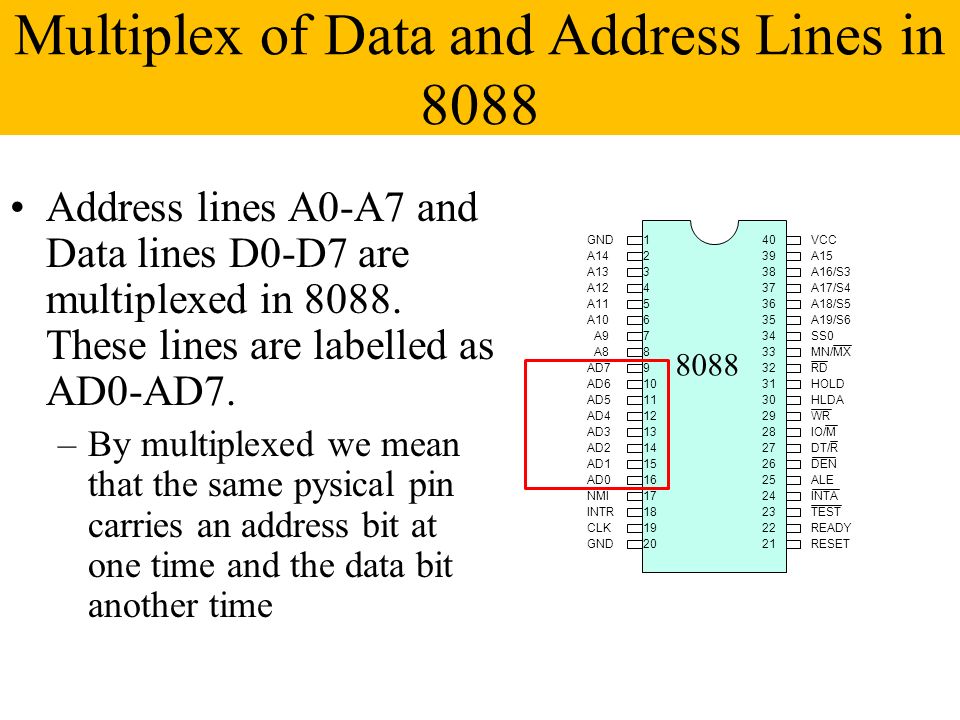
Multiplex of Data and Address Lines in 8088 Address lines A0-A7 and Data lines D0-D7 are multiplexed in 8088. These lines are labelled as AD0-AD7. –By multiplexed we mean that the same pysical pin carries an address bit at one time and the data bit another time

3
Multiplex of Data and Address Lines in 8086 Address lines A0-A15 and Data lines D0-D15 are multiplexed in 8086. These lines are labelled as AD0-AD15.

4
Minimum-mode and Maximum-mode Systems 8088 and 8086 microprocessors can be configured to work in either of the two modes: the minimum mode and the maximum mode Minimum mode: Pull MN/MX to logic 1 Typically smaller systems and contains a single microprocessor Cheaper since all control signals for memory and I/O are generated by the microprocessor. Maximum mode Pull MN/MX logic 0 Larger systems with more than one processor (designed to be used when a coprocessor (8087) exists in the system) Lost Signals in Max Mode
 exists in the system) Lost Signals in Max Mode.")
5
Minimum-mode and Maximum-mode Signals GND AD14 AD13 AD12 AD11 AD10 AD9 AD8 AD7 AD6 AD5 AD4 AD3 AD2 AD1 AD0 NMI INTR CLK GND VCC AD15 A16/S3 A17/S4 A18/S5 A19/S6 RQ/GT0 RQ/GT1 QS0 READY RESET BHE/S7 MN/MX RD LOCK S2 S1 S0 QS1 TEST 1 2 3 4 5 6 7 8 9 10 11 12 13 14 15 16 17 18 19 20 31 30 29 28 27 26 25 24 23 22 21 40 39 38 37 36 35 34 33 32 8086 Max ModeMin Mode Vcc GND

6
8086 System Minimum mode

7
8086 System Maximum Mode

8
Description of the Pins GND AD14 AD13 AD12 AD11 AD10 AD9 AD8 AD7 AD6 AD5 AD4 AD3 AD2 AD1 AD0 NMI INTR CLK GND VCC AD15 A16/S3 A17/S4 A18/S5 A19/S6 RQ/GT0 RQ/GT1 QS0 READY RESET BHE/S7 MN/MX RD LOCK S2 S1 S0 QS1 TEST 1 2 3 4 5 6 7 8 9 10 11 12 13 14 15 16 17 18 19 20 31 30 29 28 27 26 25 24 23 22 21 40 39 38 37 36 35 34 33 32 8086 Max ModeMin Mode Vcc GND

9
CPU componentContents FlagsCleared Instruction Pointer0000H CSFFFFH DS, SS and ES0000H QueueEmpty RESET Operation results

10
S2S1S0 Characteristics 000 Interrupt acknowledge 001 Read I/O port 010 Write I/O port 011 Halt 100 Code access 101 Read memory 110 Write memory 111 Passive State S0, S1 and S2 Signals

11
QS1 Characteristics 0 0No operation 0 1First byte of opcode from queue 1 0Empty the queue 1 1Subsequent byte from queue QS1 and QS2 Signals

12
IO/MDT/RSSOCHARACTERISTICS 000Code Access 001Read Memory 010Write Memory 011Passive 100Interrupt Acknowledge 101Read I/O port 110Write I/O port 111Halt Read Write Control Signals

13
TIMING SEQUENCE AN EXTERNAL CLOCK GENERATOR DEVICE IS CONNECTED TO 8086 TO PROVIDE CLOCK SIGNALS THROUGHOUT THE SYSTEM. ONE CYCLE OF CLOCK IS CALLED A STATE OR T- STATE. EACH BASIC OPERATION SUCH AS READING A MEMORY LOCATION OR WRITING TO A PORT REQUIRES SEVERAL STATES.THIS GROUP OF STATES IS CALLED A MACHINE CYCLE. THE TOTAL TIME REQUIRED TO FETCH AND EXECUTE AN INSTRUCTION IS CALLED AN INSTRUCTION CYCLE. AN INSTRUCTION CYCLE CONSISTS OF ONE OR MORE MACHINE CYCLE.

14
BASIC SIGNAL FLOW ON 8086 BUSES BASICALLY THERE ARE TWO OPERATIONS TO SEE: 1.READ OPERATION 2. WRITE OPERATION WILL SEE WHAT IS GOING ON DURING THIS TWO CYCLES OF OPERATION.

15
READ CYCLE HERE WE WILL SEE THE ACTIVITIES CARRIED OUT ON 8086 BUSES AT VARIOUS TIME INSTANTS WHEN IT READS FROM A MEMORY LOCATION OR FROM A PORT. HERE WE WILL ASSUME THAT THE 8086 IS OPERATED IN IS MINIMUM MODE.

16
CLK M/IO ALE ADDR/ DATA ADDR/ STATUS RD/INTA READY DT/R DEN T1T2T3TWTW T4 A15-A0 A19-A16 RESERVED FOR DATA VALID D15-D0 MEMORY ACCESS TIME

17
WRITE CYCLE HERE WE WILL SEE THE ACTIVITIES CARRIED OUT ON 8086 BUS AT VARIOUS TIME INSTANTS WHEN IT WRITES TO A PORT OR A MEMORY LOCATION. HERE WE WILL ASSUME THAT THE 8086 IS OPERATED IN IS MINIMUM MODE.

18
CLK M/IO ALE ADDR/ DATA ADDR/ STATUS READY DT/R DEN T1T2T3TWTW T4 A15-A0 A19-A16 DATA OUT (D15-D0) WR
 WR")
19
Data can be accessed from the memory in four different ways: 8 - bit data from Lower (Even) address Bank. 8 - bit data from Higher (Odd) address Bank. 16 - bit data starting from Even Address. 16 - bit data starting from Odd Address. 8086 Memory Addressing
 address Bank bit data starting from Even Address bit data starting from Odd Address Memory Addressing.")
20
Treating Even and Odd Addresses

21
8-bit data from Even address Bank MOVSI,4000H MOVAL,[SI+2]
![8-bit data from Even address Bank MOVSI,4000H MOVAL,[SI+2]](http://images.slideplayer.com/32/10006069/slides/slide_21.jpg "8-bit data from Even address Bank MOVSI,4000H MOVAL,[SI+2]")
22
8-bit Data from Odd Address Bank MOVSI,4000H MOVAL,[SI+3]
![8-bit Data from Odd Address Bank MOVSI,4000H MOVAL,[SI+3]](http://images.slideplayer.com/32/10006069/slides/slide_22.jpg "8-bit Data from Odd Address Bank MOVSI,4000H MOVAL,[SI+3]")
23
16-bit Data Access starting from Even Address MOVSI,4000H MOVAX,[SI+2]
![16-bit Data Access starting from Even Address MOVSI,4000H MOVAX,[SI+2]](http://images.slideplayer.com/32/10006069/slides/slide_23.jpg "16-bit Data Access starting from Even Address MOVSI,4000H MOVAX,[SI+2]")
24
16-bit Data Access starting from Odd Address MOVSI,4000H MOVAX,[SI+5]
![16-bit Data Access starting from Odd Address MOVSI,4000H MOVAX,[SI+5]](http://images.slideplayer.com/32/10006069/slides/slide_24.jpg "16-bit Data Access starting from Odd Address MOVSI,4000H MOVAX,[SI+5]")
25
Read Timing Diagram

26
Write Machine Cycle

27
INTR is used to request a hardware interrupt. It is recognized by the processor only when IF = 1, otherwise it is ignored (STI instruction sets this flag bit). The request on this line can be disabled (or masked) by making IF = 0 (use instruction CLI) If INTR becomes high and IF = 1, the 8086 enters an interrupt acknowledge cycle (INTA becomes active) after the current instruction has completed execution. INTR (input) Hardware Interrupt Request Pin
. The request on this line can be disabled (or masked) by making IF = 0 (use instruction CLI) If INTR becomes high and IF = 1, the 8086 enters an interrupt acknowledge cycle (INTA becomes active) after the current instruction has completed execution. INTR (input) Hardware Interrupt Request Pin.")
28
If I/O peripheral wants to interrupt the processor, the “interrupt controller” will send high pulse to the 8086 INTR pin. What about if a simple system to be built and hardware interrupts are not needed; What to do with INTR and INTA? For Discussion

29
The Non Maskable Interrupt input is similar to INTR except that the NMI interrupt does not check to see if the IF flag bit is at logic 1. This interrupt cannot be masked (or disabled) and no acknowledgment is required. It should be reserved for “catastrophic” events such as power failure or memory errors. NMI (input) Non-Maskable Interrupt line
 and no acknowledgment is required. It should be reserved for catastrophic events such as power failure or memory errors. NMI (input) Non-Maskable Interrupt line.")
30
8086 External Interrupt Connections NMI - Non-Maskable InterruptINTR - Interrupt Request Interrupt Logic int into Divide Error Single Step NMI Requesting Device 8086 CPU Intel 8259A PIC NMI INTR SoftwareTraps Programmable Interrupt Controller (part of chipset)
")
31
The TEST pin is an input that is tested by the WAIT instruction. If TEST is at logic 0, the WAIT instruction functions as a NOP. If TEST is at logic 1, then the WAIT instruction causes the 8086 to idle, until TEST input becomes a logic 0. This pin is normally driven by the 8087 co- processor (numeric coprocessor). This prevents the CPU from accessing a memory result before the NDP has finished its calculation TEST (input)
. This prevents the CPU from accessing a memory result before the NDP has finished its calculation TEST (input).")
32
This input is used to insert wait states into processor Bus Cycle. If the READY pin is placed at a logic 0 level, the microprocessor enters into wait states and remains idle. If the READY pin is placed at a logic 1 level, it has no effect on the operation of the processor. It is sampled at the end of the T2 clock pulse Usually driven by a slow memory device Ready (input)
.")
33
CLK Ready Reset + 5 V R C RES X1 X2 F/C RDY1 RDY2 8284 AEN1 AEN2 RESET KEY 8086 Microprocessor 8284 Connected to 8086 Mp

34
The HOLD input is used by DMA controller to request a Direct Memory Access (DMA) operation. If the HOLD signal is at logic 1, the microprocessor places its address, data and control bus at the high impedance state. If the HOLD pin is at logic 0, the microprocessor works normally. HOLD (input)
.")
35
Hold acknowledge is made high to indicate to the DMA controller that the processor has entered hold state and it can take control over the system bus for DMA operation. HLDA (output) Hold Acknowledge Output
 Hold Acknowledge Output.")
36
DMA Operation

Similar presentations

![8086 [2] Ahad. Internal! External? 8086 vs 8088 16_bit Data Bus 20_bit Address 8_bit Data Bus 20_bit Address 8088 8086 Only external bus of 8088 is.](/11/3255261/big_thumb.jpg "8086 [2] Ahad. Internal! External? 8086 vs 8088 16_bit Data Bus 20_bit Address 8_bit Data Bus 20_bit Address 8088 8086 Only external bus of 8088 is.>")


 is needed. Sources of interrupts: internal fault (e.g.. divide by.>")

