Download presentation
Presentation is loading. Please wait.

1
Frequency Limits of InP-based Integrated Circuits rodwell@ece.ucsb.edu 805-893-3244, 805-893-5705 fax Collaborators (III-V MOS) A. Gossard, S. Stemmer, C. Van de Walle University of California Santa Barbara P. Asbeck, A. Kummel, Y. Taur, University of California San Diego J. Harris, P. McIntyre, Stanford University C. Palmstrøm, University of Minnesota M. Fischetti University of Massachusetts Amherst Plenary, Indium Phosphide and Related Materials Conference, May 15-18, Matsue, Japan Sponsors J. Zolper, S. Pappert, M. Rosker DARPA (TFAST, SWIFT, FLARE) D. Purdy, I. Mack Office of Naval Research Kwok Ng, Jim Hutchby Semiconductor Research Corporation Mark Rodwell, E. Lind, Z. Griffith, S. R. Bank, A. M. Crook U. Singisetti, M. Wistey, G. Burek, A.C. Gossard University of California, Santa Barbara Collaborators (HBT) M. Urteaga, R. Pierson, P. Rowell, M-J Choe, B. Brar Teledyne Scientific Company X. M. Fang, D. Lubyshev, Y. Wu, J. M. Fastenau, W.K. Liu International Quantum Epitaxy, Inc. S. Mohney Penn State University
 D. Purdy, I. Mack Office of Naval Research Kwok Ng, Jim Hutchby Semiconductor Research Corporation Mark Rodwell, E. Lind, Z. Griffith, S. R. Bank, A. M. Crook U. Singisetti, M. Wistey, G. Burek, A.C. Gossard University of California, Santa Barbara Collaborators (HBT) M. Urteaga, R. Pierson, P. Rowell, M-J Choe, B. Brar Teledyne Scientific Company X. M. Fang, D. Lubyshev, Y. Wu, J. M. Fastenau, W.K. Liu International Quantum Epitaxy, Inc. S. Mohney Penn State University.")
2
Specific Acknowledgements (Prof.) Erik Lind 125 nm HBTs process technology theory / epi design Dr. Zach Griffith 500 & 250 nm HBTs 150 GHz Logic 100 GHz op-amps Dr. Mark Wistey InGaAs MOSFET process technology theory / epi design

3
THz Transistors are coming soon; both InP & Silicon InP Bipolars: 250 nm generation: → 780 GHz f max, 424 GHz f , 4-5 V BV CEO 125 nm & 62 nm nodes → ~THz devices IBM IEDM '06: 65 nm SOI CMOS → 450 GHz f max, ~1 V operation Intel Jan '07: 45 nm / high-K / metal gate continued rapid progress → continued pressure on III-V technologies If you can't beat them, join them ! unclear if Si MOSFETs will work well at sub-22-nm gate length InGaAs/InAs/InP channels under serious investigation for CMOS VLSI. Datta, DelAlamo, Sadana,... Z. Griffith

4
THz InP vs. near-THz CMOS: different opportunities 65 / 45 / 33 / 22... nm CMOS vast #s of very fast transistors... having low breakdown, sloppy DC parameters what NEW mm-wave applications will this enable ? massive monolithic mm-wave arrays → 1 Gb/s over ~1 km mm-wave MIMO DC parameters limit analog precision...

5
THz InP vs. near-THz CMOS: different opportunities InP HBT: THz bandwidths, good breakdown, analog precision 340 GHz, 70 mW amplifiers (design) In future: 700 or 1000 GHz amplifiers ? & 200 GHz digital logic (design) In future: 450 GHz clock rate ? 30-50 GHz gain-bandwidth op-amps→ low IM3 @ 2 GHz In future: 200 GHz op-amps for low-IM3 10 GHz amplifiers? Z. Griffith M. Urteaga (Teledyne) Z. Griffith M. Jones
 In future: 700 or 1000 GHz amplifiers . & 200 GHz digital logic (design) In future: 450 GHz clock rate GHz gain-bandwidth op-amps→ low 2 GHz In future: 200 GHz op-amps for low-IM3 10 GHz amplifiers. Z. Griffith M. Urteaga (Teledyne) Z. Griffith M. Jones.")
6
Transistor Benchmarks f max matters no gain above 218 GHz Tuned amplifiers: f max sets bandwidth Mixed-signal: C cb V/ I c, C je V/ I c, R ex I c V, R bb I c V, f BVCEO is not the only voltage limit ! Need Safe Operating Area...at least BV ceo /2 at J max /2 thermal resistance, high-current breakdown high-temperature operation (~75 C) ? Goal is >1 THz f and f max <50 fs C V / I charging delays → emphasize InP-collector DHBTs
 . Goal is >1 THz f and f max <50 fs C V / I charging delays → emphasize InP-collector DHBTs.")
7
HBT Scaling Laws

9
InP DHBTs: May 2007 250-300nm 600nm 300-400nm

10
HBT Scaling Roadmaps

11
emitter 500 nm width 16 m 2 contact base 300 width, 20 m 2 contact collector 150 nm thick, 5 mA/ m 2 current density 5 V, breakdown f 400 GHz f max 500 GHz power amplifiers 250 GHz digital clock rate 160 GHz (static dividers) 2005: InP DHBTs @ 500 nm Scaling Generation ✓ ✓ ✓ ✓ ✓ ✓ ✓ ✓ ✓ ✓ ✓ (178 GHz) (150 GHz)
 2005: InP 500 nm Scaling Generation ✓ ✓ ✓ ✓ ✓ ✓ ✓ ✓ ✓ ✓ ✓ (178 GHz) (150 GHz)")
12
emitter500 250 nm width 16 9 m 2 access base300 150 width, 20 10 m 2 contact collector150 100 nm thick, 5 10 mA/ m 2 current density 5 3.5 V, breakdown f 400 500 GHz f max 500 700 GHz power amplifiers 250 350 GHz digital clock rate 160 230 GHz (static dividers) 2006: 250 nm Scaling Generation, 1.414:1 faster ✓ ✓ ✓ ✓ ✓ ✓ ✓ ✓ ✓ (425 GHz) (780 GHz)
 2006: 250 nm Scaling Generation, 1.414:1 faster ✓ ✓ ✓ ✓ ✓ ✓ ✓ ✓ ✓ (425 GHz) (780 GHz)")
13
emitter500250 125 nm width 16 9 4 m 2 access base300 150 75 width, 20 10 5 m 2 contact collector150 100 75 nm thick, 5 10 20 mA/ m 2 current density 5 3.5 3 V, breakdown f 400500 700 GHz f max 500 700 1000 GHz power amplifiers 250 350 500 GHz digital clock rate 160 230 330 GHz (static dividers) 2007: 125 nm Scaling Generation → almost-THz HBT ✓ ✓ ✓ ✓ ✓ ✓ ✓
 2007: 125 nm Scaling Generation → almost-THz HBT ✓ ✓ ✓ ✓ ✓ ✓ ✓")
14
emitter500250125 63 nm width 16 94 2.5 m 2 access base300 15075 70 nm width, 20 105 5 m 2 contact collector150 10075 53 nm thick, 5 1020 35 mA/ m 2 current density 5 3.53 2.5 V, breakdown f 400500 700 1000 GHz f max 500 700 1000 1500 GHz power amplifiers 250 350 500 750 GHz digital clock rate 160 230 330 450 GHz (static dividers) 2008-9: 65 nm Scaling Generation→beyond 1-THz HBT ✓ ✓
 : 65 nm Scaling Generation→beyond 1-THz HBT ✓ ✓")
15
HBT Scaling Challenges

16
Scaling challenges: What looks easy, what looks hard ? key device parameterrequired change collector depletion layer thicknessdecrease 2:1 base thicknessdecrease 1.414:1 emitter junction widthdecrease 4:1 collector junction widthdecrease 4:1 emitter resistance per unit emitter areadecrease 4:1 current densityincrease 4:1 base contact resistivity (if contacts lie above collector junction) decrease 4:1 base contact resistivity (if contacts do not lie above collector junction) unchanged Hard: Thermal resistance (ICs) Emitter contact + access resistance Yield in deep submicron processes Contact electromigration (?), dark-line defects (?) Probably not as hard : Maintaining adequate breakdown for 3 V operation...
 decrease 4:1 base contact resistivity (if contacts do not lie above collector junction) unchanged Hard: Thermal resistance (ICs) Emitter contact + access resistance Yield in deep submicron processes Contact electromigration ( ), dark-line defects ( ) Probably not as hard : Maintaining adequate breakdown for 3 V operation....")
17
Temperature Rise: Transistor, Substrate, Package

18
HBTs: 500 nm Generation

19
500 nm Generation in Manufacturing: Teledyne Self-aligned Dielectric Sidewall Process Emitter Contact Base Contact Dielectric Sidewall f = 405GHz f max = 392 GHz RF Gains J E = 6.5 mA/um 2 V CE = 1.5 V No short-circuits from liftoff defects. Emitter can be much thinner → small etch undercut. M. Urteaga et al, 2004 IEEE Device Research Conference, June 21-23, 2004 Electroplate emitter contact Etch emitter semiconductor Dielectric sidewall deposition Base contact patterning Selectively deposit base metal c.f. also Minh Le et al IEDM 2006 (Vitesse)
.")
20
Example ICs in 500 nm HBT 142 GHz, 800 mW master/slave latch mesa HBT UCSB sidewall /pedestal HBT Teledyne 128 GHz, 206 mW master/slave latch 175 GHz, 7.5 mW medium-power amp. mesa HBT UCSB Other Results: 160 Gb/s multiplexer (T. Swahn et al, Chalmers / Vitesse) ~5000-HBT direct-digital frequency synthesis ICs (Vitesse, Teledyne) V. Paidi Z. Griffith M. Urteaga P. Rowell D. Pierson B. Brar
 ~5000-HBT direct-digital frequency synthesis ICs (Vitesse, Teledyne) V. Paidi Z. Griffith M. Urteaga P. Rowell D. Pierson B. Brar.")
21
HBTs: 250 nm Generation

22
250 nm scaling generation InP DHBTs Emitter contact resistance 5 m 2 Base contact resistance is < 5 m 2 Z. Griffith E. Lind

23
DHBTs: 250 nm Scaling Generation 150 nm thick collector60 nm thick collector Emitter access: 5.1 m 2 Base contact: 6.3 m 2 Z. Griffith E. Lind

24
Example IC Designs in 250 nm HBT 200 GHz master-slave latches...fabrication on hold... 340 GHz, 70 mW, medium-power amplifiers...fabrication planned summer/fall 2007 M. Jones Z. Griffith

25
125 nm InP HBT development

26
Emitter Access Resistance 125 nm generation requires 5 - μm 2 emitter resistivities 65 nm generation requires 1-2 - μm 2 Recent Results: ErAs/Mb MBE in-situ1.5 - μm 2 Mb MBE in-situ 0.6 - μm 2 TiPdAu ex-situ 0.5 - μm 2 TiW ex-situ 0.7 - μm 2 Degeneracy contributes 1 - μm 2 20 nm emitter-base depletion layer contributes 1 - μm 2 resistance T e =0 nm T e =100 nm Erik Lind Adam Crook Seth Bank Uttam Singisetti 10 nm steps

27
Epitaxial Layer Development for 125 nm Generation InGaAs base: low sheet resistivity, low transit time, but collector must be graded low-current breakdown dominated by tunneling in setback layer Erik Lind 1) less superlattice periods... 2) thinner (sub-monolayer) superlattice periods → random alloy grade 3) thin GaAs/InGaAs strained-layer grade DC data shows expected increase in breakdown. Transport (RF) data is pending. : Zach Griffith B-C grade redesign: thin the setback, thin the grade calculation
 thinner (sub-monolayer) superlattice periods → random alloy grade 3) thin GaAs/InGaAs strained-layer grade DC data shows expected increase in breakdown. Transport (RF) data is pending. : Zach Griffith B-C grade redesign: thin the setback, thin the grade calculation.")
28
125 nm Emitter Process Blanket sputter deposition TiW emitter contact metal Optical lithography → ICP reactive-ion etching ICP RIE etch of InGaAs/InP semiconductor, Selective wet etch to base Erik Lind 125 nm emitter500 nm undercut at emitter ends 61 nm junction: 40 nm lateral undercut

29
UCSB 125 nm DHBT Development 125 nm emitter process Emitter Metal InGaAs/InP emitter contact resistivity ~ 0.7 - μm 2 base contact resistivity ~ 3-5 -μm 2 Target performance ~ 700-900 GHz simultaneous f t & f max, 3-4 V breakdown Erik Lind Adam Crook

30
How might we build the 62.5 nm HBT ? Mesa process: control of etch undercut with dry+wet process Alternatives: - dielectric sidewall process - sidewall process with extrinsic base regrowth: allows thinner base

31
InP-based FETs; MOSFETs & HEMTs

32
InP-based HEMTs & MOSFETs : Why ? A ~2.5:1 f / f signal ratio provides 3 dB noise figure. Low-noise 100-300 GHz preamplification is a key application for 1-THz-f HEMTs InGaAs/InP HEMTs: mm-wave low-noise amplifiers InGaAs/InP MOSFETs: post-22-nm VLSI (?) Higher mobility and peak electron velocity than in Silicon → higher ( I d / W g ) and lower ( C V / I ) at sub-22-nm scaling (?)
 Higher mobility and peak electron velocity than in Silicon → higher ( I d / W g ) and lower ( C V / I ) at sub-22-nm scaling ( ).")
35
Some Encouraging Initial Data... -- non-parabolic bands (variable m*) significantly increase feasible sheet charge Asbeck / Fischetti / Taur simulate drive currents much larger than for constant-m* model -- mobilities seem to be acceptable even in thin wells M. Wistey preliminary data... and our current device designs... device design and fabrication: Asbeck group: UCSD Taur group: UCSD Fischetti group: U. Mass Rodwell group: UCSB Palmstrøm group: U. Minn well: 2.5 nm InGaAs, 2.5 nm InP N+ InGaAs/InAs extrinsic source & drain by regrowth
 significantly increase feasible sheet charge Asbeck / Fischetti / Taur simulate drive currents much larger than for constant-m* model -- mobilities seem to be acceptable even in thin wells M. Wistey preliminary data... and our current device designs... device design and fabrication: Asbeck group: UCSD Taur group: UCSD Fischetti group: U. Mass Rodwell group: UCSB Palmstrøm group: U. Minn well: 2.5 nm InGaAs, 2.5 nm InP N+ InGaAs/InAs extrinsic source & drain by regrowth.")
36
Frequency Limits of InP-based Integrated Circuits Scaling limits: contact resistivities, device and IC thermal resistances. InP Bipolar Transistors 62 nm (1 THz f , 1.5 THz f max ) scaling generation is feasible. 700 GHz amplifiers, 450 GHz digital logic Is the 32 nm (1 THz amplifiers) generation feasible ? InP Field-Effect Transistors Low electron effective mass → difficulties with further scaling Guarded optimism regarding 22 nm generation for VLSI Serious difficulties beyond.
 scaling generation is feasible. 700 GHz amplifiers, 450 GHz digital logic Is the 32 nm (1 THz amplifiers) generation feasible . InP Field-Effect Transistors Low electron effective mass → difficulties with further scaling Guarded optimism regarding 22 nm generation for VLSI Serious difficulties beyond..")
37
(end)
")
38
non-animated versions of the three key scaling slides

39
HBT scaling laws Goal: double transistor bandwidth when used in any circuit → keep constant all resistances, voltages, currents → reduce 2:1 all capacitances and all transport delays → thin base ~1.414:1 → thin collector 2:1 → reduce junction areas 4:1 → reduce emitter contact resistivity 4:1 (current remains constant, as desired ) → reduce base contact resistivity 4:1 reduce widths 2:1 & reduce length 2:1 → constant R bb reducing widths 4:1, keep constant length → reduced R bb need to reduce junction areas 4:1 reduce widths 2:1 & reduce length 2:1 → doubles T reducing widths 4:1, keep constant length→ small T increase ✓ ✓ ✓✓ Linewidths scale as the inverse square of bandwidth because thermal constraints dominate.
 → reduce base contact resistivity 4:1 reduce widths 2:1 & reduce length 2:1 → constant R bb reducing widths 4:1, keep constant length → reduced R bb need to reduce junction areas 4:1 reduce widths 2:1 & reduce length 2:1 → doubles T reducing widths 4:1, keep constant length→ small T increase ✓ ✓ ✓✓ Linewidths scale as the inverse square of bandwidth because thermal constraints dominate.")
40
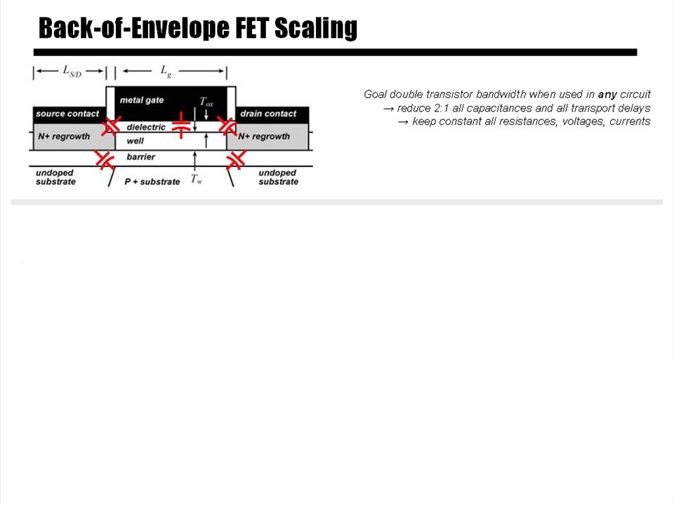
Back-of-Envelope FET Scaling (non-degenerate) c eq doubled thin layers 2:1 Goal double transistor bandwidth when used in any circuit → reduce 2:1 all capacitances and all transport delays → keep constant all resistances, voltages, currents ✓ g m, I d held constant reduce W g 2:1 ✓ C gs reduced 2:1 dielectricfringing ✓ (C gd, C s-b, C d-b ) all reduced 2:1 reduce L g 2:1 ✓ (R s, R d ) held constant reduce L s/d 2:1,reduce c 4:1 2:1 vertical scaling → 2:1 increased ( g m / W g ) → 2:1 reduced W g → 2:1 reduced fringing capacitances
 c eq doubled thin layers 2:1 Goal double transistor bandwidth when used in any circuit → reduce 2:1 all capacitances and all transport delays → keep constant all resistances, voltages, currents ✓ g m, I d held constant reduce W g 2:1 ✓ C gs reduced 2:1 dielectricfringing ✓ (C gd, C s-b, C d-b ) all reduced 2:1 reduce L g 2:1 ✓ (R s, R d ) held constant reduce L s/d 2:1,reduce c 4:1 2:1 vertical scaling → 2:1 increased ( g m / W g ) → 2:1 reduced W g → 2:1 reduced fringing capacitances")
41
FETs no longer scale well tunneling through oxide → high-K dielectrics (if feasible) Low density of states limits drive current density-of-states term dominates, limits ( g m / W g )and ( I d / W g ) → fringing & substrate capacitances no longer scale, can dominate over C gs Solomon & Laux, 2001 IEDM Thin layers & low effective mass limit channel sheet charge density high sheet-charge in thin well → populate higher-mass band minima infinite well approximation Thin quantum wells have low mobility Li SST 2005; Gold et al, SSC 1987; Sakaki et al, APL 1987
 Low density of states limits drive current density-of-states term dominates, limits ( g m / W g )and ( I d / W g ) → fringing & substrate capacitances no longer scale, can dominate over C gs Solomon & Laux, 2001 IEDM Thin layers & low effective mass limit channel sheet charge density high sheet-charge in thin well → populate higher-mass band minima infinite well approximation Thin quantum wells have low mobility Li SST 2005; Gold et al, SSC 1987; Sakaki et al, APL 1987")
42
InP DHBT: 500 nm Scaling Generation 600 nm wide emitter, 120 nm thick collector, 30 nm thick base Z. Griffith

Similar presentations

 Sub-mm-Wave ICs 805-893-3244, 805-893-5705 fax The 11th International Symposium on.>")


