Download presentation
Presentation is loading. Please wait.

1
Design of Digital-to-Analog Converter Qin Chen Yong Wang Dept. of Electrical Engineering Mar. 14th, 2006 EE597G Presentation:

2
Outline CMOS switch design and simulation Challenge and Solution R-2R Voltage DAC Schematic design and simulation results Chip Specifications Project Progress

3
CMOS Switch Circuit

4
Turn on resistance Control signal is high: When Vin<Vdd-Vgs1, M1 is turned on; When Vgs2<Vin<Vdd, M2 is turned on; The total parallel resistance make the turn-on resistance always low at the whole voltage range.

5
Simulation Results VG=0V, RL=10k Ohm VG=+5V, RL=10k Ohm

7
Challenge For R-2R current DAC, how to change virtual ground to 2.5V in CMOS circuits? How to get rid of glitches? How to implement large resistors (>10k ohm) in layout? [next step]
 in layout. [next step].")
8
Glitches in DAC output voltages Switches in DAC operate at different speeds ⇒ output glitches occur when several input bits change together: 0111->1000 Glitches are very noticeable on a video display:

9
Voltage-Mode R-2R Network DAC

10
Advantages and Disadvantages of Voltage R-2R DAC Advantages: the constant output impedance, which eases the stabilization of any amplifier connected to the output node. No glitch, switch the arms of the ladder between low impedances, capacitive glitch currents tend not to flow in the load. Disadvantages: operate over a wide voltage range (VREF to GND). This is difficult from a design and manufacturing viewpoint gain of the DAC cannot be adjusted by means of a resistor in series with the VREF terminal.
. This is difficult from a design and manufacturing viewpoint gain of the DAC cannot be adjusted by means of a resistor in series with the VREF terminal..")
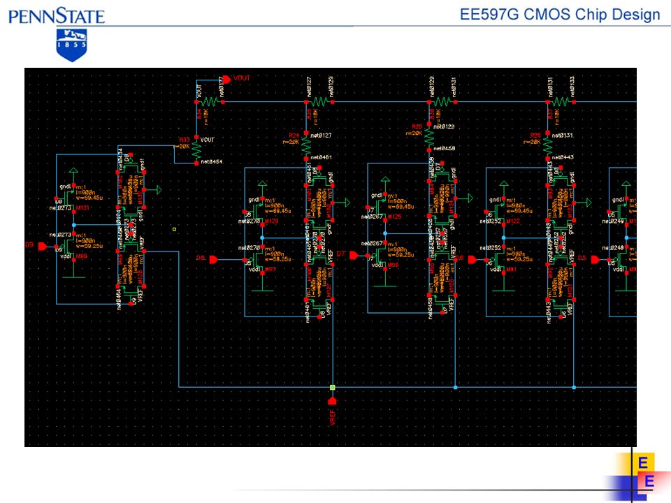
12
D9-D0: 10,0000,0000 Vref: +5V

13
Linear output characterization

14
Testing the op amp

15
Freq. Response of Gain & Phase

16
Compensation

17
Compensation result

18
Output buffer

19
The output curve of output buffer

20
Voltage Reference

21
Characteristics of voltage reference R load ( Ω )5K (I) 10K (I/2) 40K (I/8) 160K (I/32) 5M (I/1024) Open V out (V)2.50482.50272.50132.5008 5V + ─ Vout=2.5V 5V 20K R load
5K (I) 10K (I/2) 40K (I/8) 160K (I/32) 5M (I/1024) Open V out (V) V + ─ Vout=2.5V 5V 20K R load")
22
Building the DAC

23
Test the DAC

24
Test result of DAC

25
What have been done OP Amp design and simulation CMOS switch design and simulation Schematic adjustment Schematic circuit design and simulation

26
Project Progress =>> Week 1Systematic design of chip Week 2Systematic design of chip (cont.) Week 3Circuit design Week 4Circuit design (cont.) Week 5Layout design Week 6Layout design (cont.) Week 7Final adjustments and verification Week 8Final adjustments and verification (cont.)
 Week 3Circuit design Week 4Circuit design (cont.) Week 5Layout design Week 6Layout design (cont.) Week 7Final adjustments and verification Week 8Final adjustments and verification (cont.)")
Similar presentations