Download presentation
Presentation is loading. Please wait.

1
Chapter 5

2
Read pages 311-337 much useful information such as common gates on page 329
Open collector Schmitt trigger

3
Programmable Logic Arrays (PLAs)
Any combinational logic function can be realized as a sum of products. Idea: Build a large AND-OR array with lots of inputs and product terms, and programmable connections. n inputs AND gates have 2n inputs -- true and complement of each variable. m outputs, driven by large OR gates Each AND gate is programmably connected to each output’s OR gate. p AND gates (p<<2n The number of minterms)
")
4
Example: 4x3 PLA, 6 product terms (Programmed by blowing fuses)
")
5
PLD’s – PLA’s page 337-345 Implement BCD to Excess-3. See page 49.

6
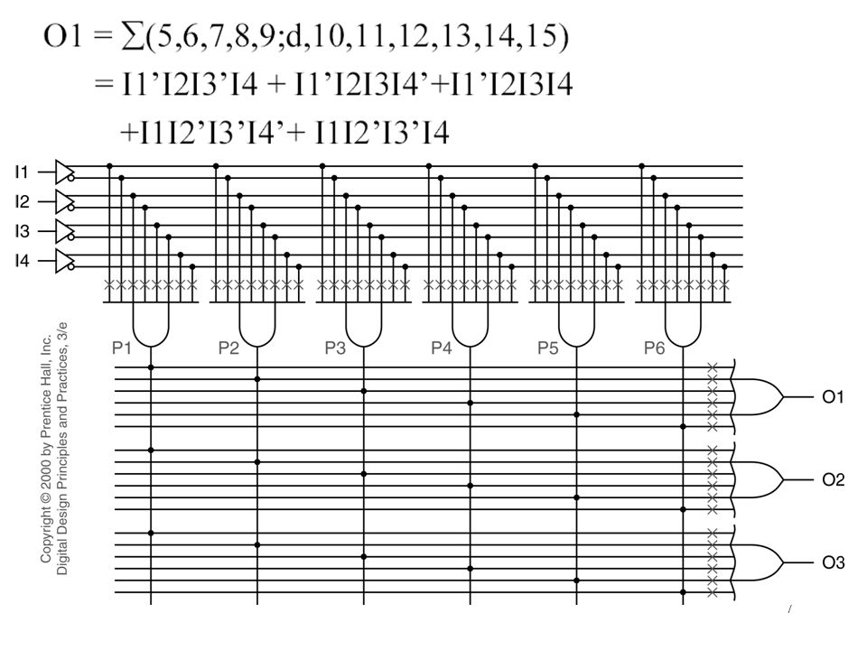
BCD to Excess-3 via PLA BCD EXCESS-3 I1 I2 I3 I4 O1 O2 O3 O4 0 0 0 0
O1 = (5,6,7,8,9;d,10,11,12,13,14,15) = I1’I2I3’I4 + I1’I2I3I4’+I1’I2I3I4 +I1I2’I3’I4’+ I1I2’I3’I4 O2 = (1,2,3,4,9;d,10,11,12,13,14,15) = I1’I2’I3’I4+ I1’I2’I3I4’+ I1’I2’I3I4+ I1I2’I3’I4’+ I1I2I3’I4’ O3 = (0,3,4,7,8;d,10,11,12,13,14,15) = I1’I2’I3’I4’+ I1’I2’I3I4+ I1’I2I3’I4’+ I1’I2I3I4+ I1I2’I3’I4’ O4 = (0,2,4,6,8;d,10,11,12,13,14,15) = I4’
 = I1’I2I3’I4 + I1’I2I3I4’+I1’I2I3I4. +I1I2’I3’I4’+ I1I2’I3’I4. O2 = (1,2,3,4,9;d,10,11,12,13,14,15) = I1’I2’I3’I4+ I1’I2’I3I4’+ I1’I2’I3I4+ I1I2’I3’I4’+ I1I2I3’I4’ O3 = (0,3,4,7,8;d,10,11,12,13,14,15) = I1’I2’I3’I4’+ I1’I2’I3I4+ I1’I2I3’I4’+ I1’I2I3I4+ I1I2’I3’I4’ O4 = (0,2,4,6,8;d,10,11,12,13,14,15) = I4’")
9
Some product terms

10
PLA Electrical Design See Section wired-AND logic

11
Programmable Array Logic (PALs)
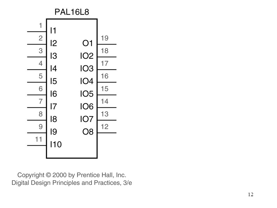
How beneficial is product sharing? Not enough to justify the extra AND array PALs ==> fixed OR array Each AND gate is permanently connected to a certain OR gate. Example: PAL16L8

13
10 primary inputs 8 outputs, with 7 ANDs per output 1 AND for 3-state enable 6 outputs available as inputs more inputs, at expense of outputs two-pass logic, helper terms Note inversion on outputs output is complement of sum-of-products newer PALs have selectable inversion

14
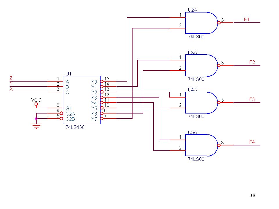
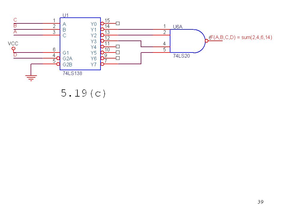
Decoders General decoder structure Typically n inputs, 2n outputs
2-to-4, 3-to-8, 4-to-16, etc.

15
Binary 2-to-4 decoder Note “x” (don’t care) notation. Y(I1, I0)
 notation. Y(I1, I0)")
16
2-to-4-decoder logic diagram
Y(I1, I0)
")
17
MSI 2-to-4 decoder Y(B, A) Input buffering (less load)
NAND gates (faster) Y(B, A)
 Y(B, A)")
18
Decoder Symbol Y(B, A)
")
19
Complete 74x139 Decoder Y(B, A)
")
20
More decoder symbols

21
3-to-8 decoder Y(C, B, A)
")
22
74x138 3-to-8-decoder symbol Y(C, B, A)
")
23
Decoder cascading Y(C, B, A) 4-to-16 decoder
 4-to-16 decoder")
24
More cascading 5-to-32 decoder

25
Decoder applications Microprocessor memory systems
selecting different banks of memory Microprocessor input/output systems selecting different devices Microprocessor instruction decoding enabling different functional units Memory chips enabling different rows of memory depending on address Lots of other applications

26
Tri-state drivers

27
Three-state buffers Output = LOW, HIGH, or Hi-Z.
Can tie multiple outputs together, if at most one at a time is enabled.

28
Different flavors

29
Only one Y can be low at a time.

30
Three-state drivers

31
Typical application of tri-state drivers – input port.
INSELn’s are a function of Address signals. They may be obtained external to the microprocessor using a decoder (74LS138).
.")
32
Three-state transceiver
Typical application – connected to microprocessor data buss to provide sufficient current drive for multiple memory and I/O (input and output) ports.
 ports.")
33
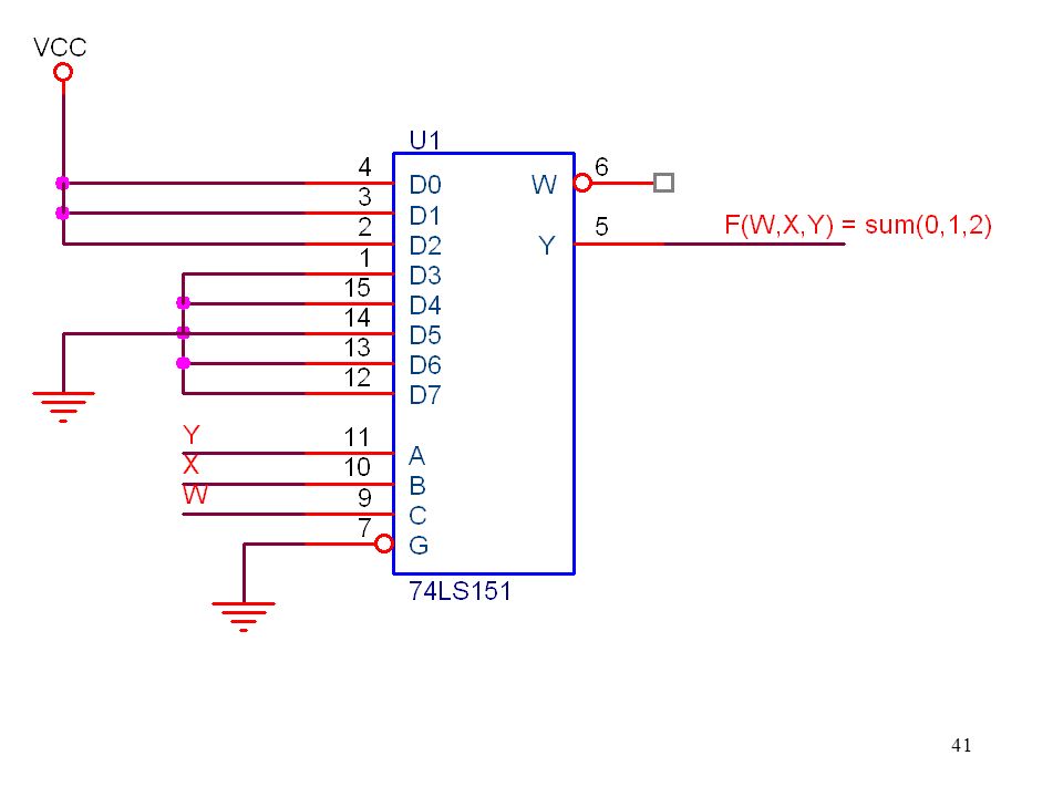
Multiplexers – many inputs to one output.

34
74x151 8-input multiplexer

35
74x151 truth table

36
Logic design using multiplexer.

40
m W X Y Z F n Dn 1 2 3 4 5 6 7 8 9 10 11 12 13 14 15 Y X W

42
Equality Comparators 1-bit comparator 4-bit comparator EQ_L

43
Adders Basic building block is “full adder”
1-bit-wide adder, produces sum and carry outputs Truth table: X Y Cin S Cout

44
Full Adder X Cout 1 Cin Y X S 1 Cin Y

45
Full-adder circuit Delay X, Y, Cin to Cout = 2. Delay X, Y to S = 2.
Delay Cin to S = 1.

46
Ripple adder Speed limited by carry chain
Delay X, Y, Cin to Cout = 2. Delay X, Y to S = 2. Delay Cin to S = 1. Speed limited by carry chain Faster adders eliminate or limit carry chain 2-level AND-OR logic ==> 2n product terms 3 or 4 levels of logic, carry lookahead (see book). Two’s complement subtraction: Invert and add 1.
. Two’s complement subtraction: Invert and add 1.")
47
Multipliers 8x8 multiplier

48
Full-adder array

49
Faster carry chain

50
Read-Only Memories

51
Why “ROM”? Program storage Boot ROM for personal computers
Program for embedded application storage for embedded systems. Actually, a ROM is a combinational circuit, basically a truth-table lookup. Can perform any combinational logic function Address inputs = function inputs Data outputs = function outputs

52
Logic-in-ROM example

53
4x4 multiplier example

54
Internal ROM structure
PDP-11 boot ROM (64 words, 1024 diodes)
")
55
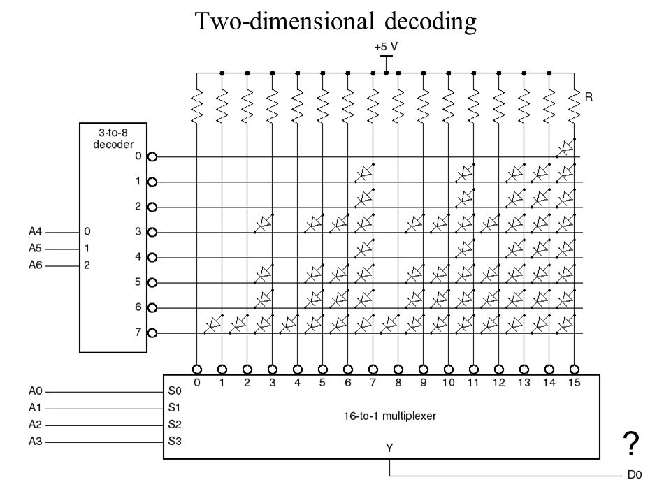
Two-dimensional decoding
?
56
Typical commercial EEPROMs

57
EEPROM programming Apply a higher voltage to force bit change
E.g., VPP = 12 V On-chip high-voltage “charge pump” in newer chips Erase bits Byte-byte Entire chip (“flash”) One block (typically 32K - 66K bytes) at a time Programming and erasing are a lot slower than reading (milliseconds vs. 10’s of nanoseconds)
 One block (typically 32K - 66K bytes) at a time. Programming and erasing are a lot slower than reading (milliseconds vs. 10’s of nanoseconds)")
58
Microprocessor EPROM application

Similar presentations


 – –a fixed array of AND gates.>")


 The slides included herein were taken.>")


