Download presentation
Presentation is loading. Please wait.

1
PIT: Programmable Interval Timer
Introduction to 8253/8254

2
8253/54 Timer Timer Description and Initialization
PIT (programmable Interval Timer) The 8253 chip was used in the IBM PC/XT, but starting with the IBM PC/AT, the 8254 replaced the 8253. 8253 and 8254 have exactly the same pinout. 8254 is a superset of the 8253.
 The 8253 chip was used in the IBM PC/XT, but starting with the IBM PC/AT, the 8254 replaced the and 8254 have exactly the same pinout is a superset of the")
3
Programmable Interval Timer - 8254

4
Pin Diagram

6
Pin Description of 8253/54 A0, A1, and CS
Inside the 8253/54 timer, there are 3 counters. Each timer works independently and programmed separately. Each counter is assigned an individual port address. The control register common to all 3 counters and has its own port.

8
CLK CLK is the input clock frequency, which can range between 0 and 2 MHz for the 8253. For input frequencies higher than 2 MHz, the 8254 must be used. The 8254 can go as high as 8 MHz, and can go 10 MHz. OUT Can have square-wave, one-shot, and other square-shape waves for various duty cycles but no sine-wave or saw-tooth shapes. Gate This pin is used to enable or disable the counter.

9
D0-D7 The D0-D7 data bus of the 8253/54 is a bidirectional bus connected to D0-D7 of the system data bus. RD and WR are connected to IOR and IOW control signals of the system bus. Initialization of the 8253/54 Each of the three counters of the 8253/54 must be programmed separately. The 8253/54 must be initialized before it is used.

14
Control word The figure shows the one-byte control word of the 8253/54. D0 chooses between a binary number divisor of 0000 to FFFFH or a BCD divisor of 0000 to 9999H. The highest number is 216 for binary and 104 for BCD. To get the highest count, the counter is loaded with zeros. D1, D2, and D3 are for mode selection.

15
D4 and D5 are for RL0 and RL1 RL0 and RL1 are used to indicate the size of the divisor, and have 3 options: Read/write MSB only Read/write LSB only Read/write LSB first followed immediately by the MSB.

16
Operation Modes Mode 0 Interrupt on terminal count
Mode 1 Programmable one-shot Mode 2 Rate Generator Mode 3 Square wave rate generator Mode 4 Software triggered strobe Mode 5 Hardware trigger strobe

17
All counters are down counters.
D6 and D7 are used to select the 3 counters, counter 0, counter 1, or counter 2, is to be initialized by the control byte. To program a given counter of the 8253/54 to divide the CLK input frequency one must send the divisor to that specific counter’s reg. To divide the frequency by (BCD) or (binary) we must send in 0 for both high and low bytes.
 or (binary) we must send in 0 for both high and low bytes.")
21
IBM PC 8253/54 Timer Connections and Programming

22
PCLK of the 8284 is 2.3863663 MHz and must be divided by 2.
The three clocks of the 8253, CLK0, CLK1, and CLK2, are all connected to a constant frequency of MHz. PCLK of the 8284 is MHz and must be divided by 2. GATE0 and GATE1 enable counter0 and counter 1 respectively. GATE2 of counter 2 can be enabled or disabled through PB0 of port B of the 8255.

24
Using counter 0 CLK0 of counter 0 is MHz, and GATE0 is connected permanently. OUT0 is connected to IRQ0 of the 8259 interrupt controller to provide time-of-day (TOD) interrupt. IRQ0 is activated 18.2 times per second. (18.2 Hz) The counter must to divide MHz by 65,536.
 interrupt. IRQ0 is activated 18.2 times per second. (18.2 Hz) The counter must to divide MHz by 65,536.")
25
Using counter 0 D0 = 0 for the binary value. D3 D2 D1 = 011, mode 3
The wave shape is a square wave. D0 = 0 for the binary value. D3 D2 D1 = 011, mode 3 D4 D5 = 11, for reading/writing the LSB first, followed by MSB. D7 D6 = 00, for counter 0.

27
Using counter 0 The function of IR0 is not only taking care of the TOD clock. BIOS will make this interrupt available by going to the vector table of INT 1CH.

28
Using Counter 1 In counter 1, CLK1 is connected to MHz and GATE is high. OUT1 generates a periodic pulse required to refresh DRAM memory of the computer. The refreshing must be done at least 15s (66278Hz) for each cell, and is performed by DMA. Counter must divide the input frequency MHz by 18. DRAM maximum frequency refresh time is 2 ms.
 for each cell, and is performed by DMA. Counter must divide the input frequency MHz by 18. DRAM maximum frequency refresh time is 2 ms.")
29
Using Counter 1 D0 = 0 for binary option
D3 D2 D1 = 010, for mode 2 shape output. D5 D4 = 01, for LSB only D7 D6, for counter 1. D7~D0 = = 54H for the control word.

30
Using Counter 2 The output of counter 2 is connected to two different devices: the speaker and PC5 of the 8255. Use of timer 2 by the speaker In the IBM PC, CLK2 is connected to a frequency of MHz and GATE2 is programmed by PB0 of port 61H (port B). The IBM PC uses counter 2 to generate the beep sound. The beep sound has a frequency of 896 Hz (divisor = 1331)
. The IBM PC uses counter 2 to generate the beep sound. The beep sound has a frequency of 896 Hz (divisor = 1331)")
32
Turning on the speaker via PB0 and PB1 of port 61H
The process of turning on the speaker is the same for all IBM PCs and compatibles from 8088-based to and Intel’s Pentium-based systems. Gate2 must be high to provide the CLK to timer 2. This function is performed by PB0 of port 61H. The following is the code to turn the speaker on.

33
Turning on the speaker via PB0 and PB1 of port 61H

34
Time delay for 80x86 PCs Creating time delays in 8088/86-based PC/XT, PS2, and compatibles MOV CX, N AGAIN: LOOP AGAIN The above codes can be used to generate delays (N T 17 seconds) Approximate delay time The delay is not only frequency dependent but also CPU dependent. IBM provides a scheme to create a time delay using hardware that is not only frequency but also CPU independent.
 Approximate delay time. The delay is not only frequency dependent but also CPU dependent. IBM provides a scheme to create a time delay using hardware that is not only frequency but also CPU independent.")
35
Time delays in 80x86 IBM PC The following method of creating hardware time delays was first implemented in the IBM PC and compatible computers. To create a processor independent delay, IBM made PB4 of port 61H toggle every s. CS holds s in the following codes.

36
Time delays in 80x86 IBM PC

37
Time delays in 80x86 IBM PC Now a time delay of any duration can be created regardless of the CPU frequency as long as it is a 286 and higher PC. For example set CX=33144 (3314415.085s=0.5 second) MOV CX, 33144 CALL WAITF
 MOV CX, CALL WAITF.")
38
Time delays in 80x86 IBM PC

39
Example

40
Examples

41
Generating Music on the IBM PC
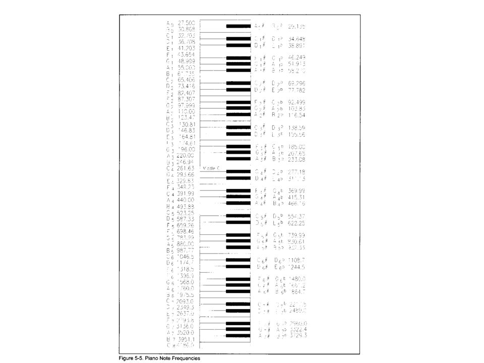
As mentioned earlier, counter 2 is connected to the speaker and it can be programmed to output any frequency that is desired. Look at the list of piano notes and their frequencies given in Fig. 5-5. Music: frequency and time duration

44
A delay of 250 ms

49
Shape of 8253/54 Outputs

50
Out0 pulse shape in IBM BIOS
IBM BIOS programmed counter 0 to create mode 3, which is square-wave shape. Counter 0 is loaded with the number 65,536 and the clock period of input frequency 838 ns (1/1.193 MHz = 838 ns), so the period of the OUT0 pulse is equal to 65536838 ns = 54.9 ms (18.2 Hz). OUT0 continuously sends out square wave pulses.
, so the period of the OUT0 pulse is equal to 65536838 ns = 54.9 ms (18.2 Hz). OUT0 continuously sends out square wave pulses.")
51
Out1 pulse shape in the IBM BIOS
IBM BIOS programmed counter 1 in mode 2, rate generator, with the value 18 loaded into the counter. OUT1 will be high for a total of 17 838 ns and go low for one pulse of 838 ns GATE1 is set to 1 permanently

52
OUT2 pulse shape in the IBM BIOS
IBM BIOS loads the value 1331 into counter 2. Since 1331 is an odd number, the OUT2 pulse is high for a total of (1331+1)/2 = 666 838 ns and is low for a total of (1331-1)/2 = 665 838 ns
/2 = 666 838 ns and is low for a total of (1331-1)/2 = 665 838 ns.")
53
Mode 0: interrupt on terminal count
The output in this mode is initially low, and will remain low for the duration of the count if GATE = 1. Width of low pulse = NT Where N is the the clock count loaded into counter, and T is the clock period of the CLK input.

54
Mode 0: interrupt on terminal count
When the terminal count is reached, the output will go high and remain high until a new control word or new count number is loaded. In this mode, if GATE input becomes low at the middle of the count, the count will stop and the output will be low. The count resumes when the gate becomes high again. This in effect adds to the total time the output is low.

58
Mode 1: programmable one-shot
This mode is also called hardware triggerable one-shot. The triggering must be done through the GATE input by sending a 0-to-1 pulse to it. The following two steps must be performed: Load the count registers. A 0-to-1 pulse must be sent to the GATE input to trigger the counter. Contrast this with mode 0, in which the counter produces the output immediately after the counter is loaded as long as GATE = 1. In mode 1 after sending the 0-to-1 pulse to GATE, OUT becomes low and stays low for a duration of NT, then becomes high and stays high until the gate is triggered again.

61
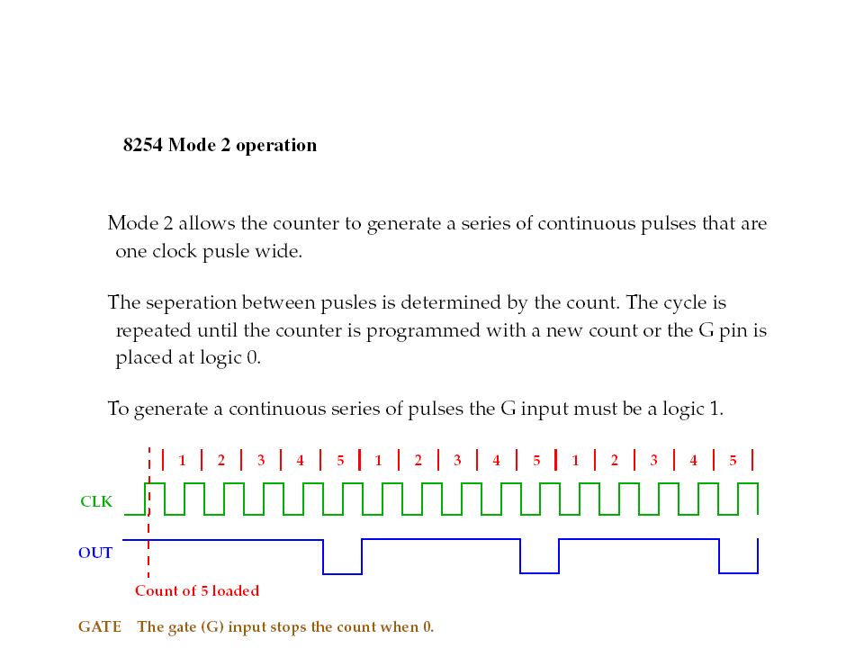
Mode 2: rate generator Mode 2 is also called divide-by-N counter.
In this mode, if GATE = 1, OUT will be high for the NT clock period, goes low for only one clock pulse, then the count is reloaded automatically, and the process continues indefinitely.

63
Mode 3: square wave rate generator
In this mode if GATE = 1, OUT is a square wave where the high pulse is equal to the low pulse if N is an even number. In this case the high part and low part of the pulse have the same duration and are equal to (N/2)T (50% duty cycle) If N is an odd number, the high pulse is one clock pulse longer. This mode is widely used as a frequency divider and audio-tone generator.
T (50% duty cycle) If N is an odd number, the high pulse is one clock pulse longer. This mode is widely used as a frequency divider and audio-tone generator.")
66
Mode 4: software trigger strobe
In this mode if GATE = 1, the output will go high upon loading the count. It will stay high for the duration of NT. After the count reaches zero (terminal count), it becomes low for one clock pulse, then goes high again and stays high until a new command word or new count is loaded. To repeat the strobe, the count must be reloaded again. Mode 4 is similar to mode 2, except that the counter is not reloaded automatically. In this mode, the count starts the moment the count is written into the counter.
, it becomes low for one clock pulse, then goes high again and stays high until a new command word or new count is loaded. To repeat the strobe, the count must be reloaded again. Mode 4 is similar to mode 2, except that the counter is not reloaded automatically. In this mode, the count starts the moment the count is written into the counter.")
70
Mode 5: hardware trigger strobe
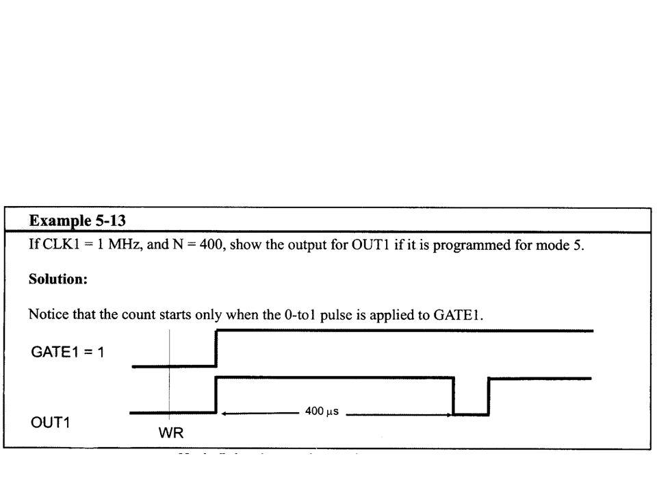
This mode is similar to mode 4 except that the trigger must be done with the GATE input. In this mode after the count is loaded, we must send a low-to-high pulse to the gate to start the counter.

Similar presentations


 Data Sheet Machine Projects –Continue on MP3 Labs –Continue in labs with your assigned.>")

, No Bidirectional.>")


 Read-Write Memory (RAM)>")
. 8254 Modes Gate is low the count will be paused Gate is high Will continue counting Mode 0: An events counter.>")
