Download presentation
Presentation is loading. Please wait.

1
Chapter 6. Bipolar Junction Transistors (BJTs)
")
2
Bipolar Junction Transistor Three terminal device Voltage between two terminals to control current flow in third terminal Invented in 1948 at Bell Telephone Laboratories Dominant until late 1980’s Reliable under harsh operating conditions –High frequency applications –High speed designs –High power applications

3
npn transistor n-type emitter (E) region, p-type base (B) region, n-type collector (C) region Two pn junctions (naming basis for bipolar junction transistor) Modes -Active: used for amplifier design -Cutoff -Saturation: used for logic design -Reverse active: limited operation
 region, p-type base (B) region, n-type collector (C) region Two pn junctions (naming basis for bipolar junction transistor) Modes -Active: used for amplifier design -Cutoff -Saturation: used for logic design -Reverse active: limited operation")
4
pnp transistor – dual of npn transistor

5
Active Mode of npn Transistor

8
Circuit Models for Active Mode npn Transistor

9
Practical Implementation E and C are not symmetrical. pnp transistors works dual to npn transistors much in the same way PMOSFET works dual to NMOSFET. (In this class, we will concentrate on npn transistors.)
.")
10
Circuit Symbols for npn Transistors Biasing in active mode Directions of current flow

12
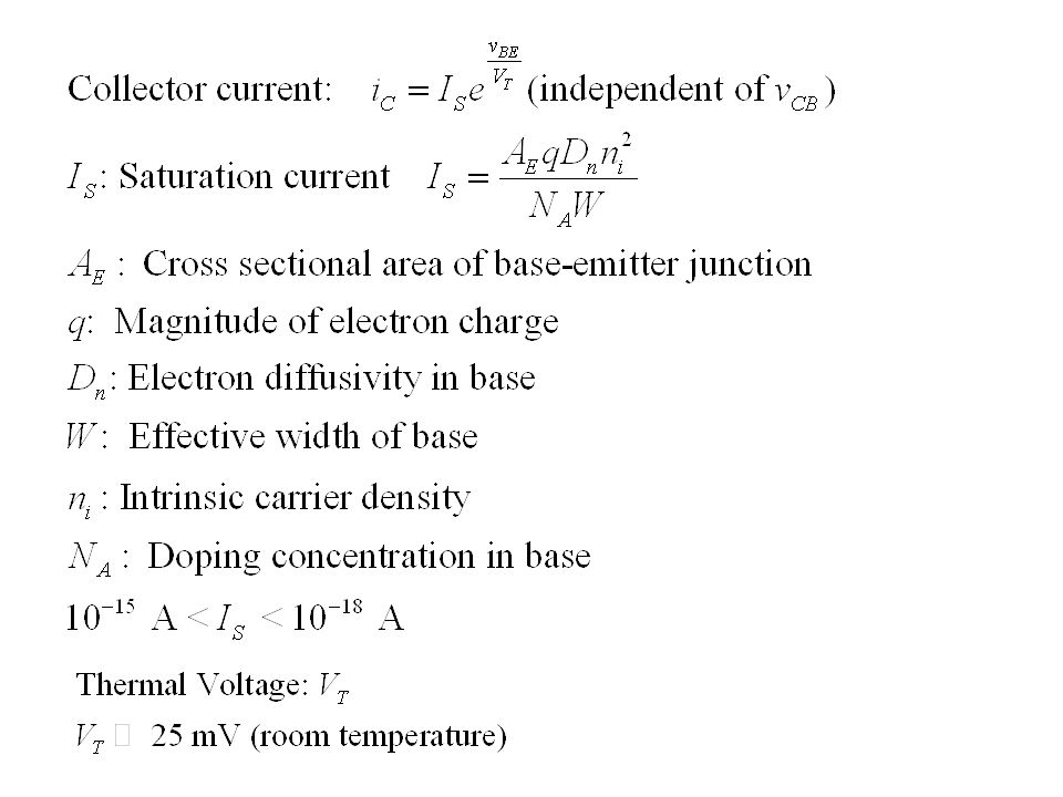
i C – v BE Characteristics Temperature Dependence

13
Common Base Characteristics Base voltage is fixed at zero. In active region, v CB ≥ - 0.4 V

14
Dependence of i C on Collector Voltage

15
Circuit Models with Output Resistance r o

16
Common Emitter Configuration

18
Common Emitter Saturation Model

19
Designing Linear Amplifiers (Active Region)
")
20
Amplifier Gain

22
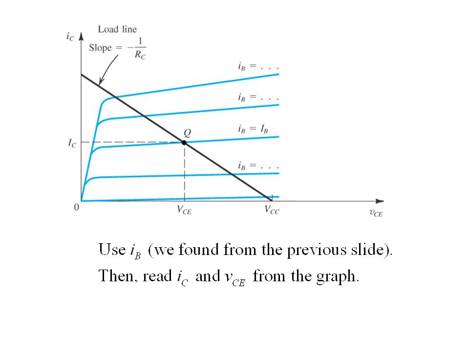
Graphical Analysis

24
To determine i B, i C and v CE, you need to use both graphs.

25
Quiescent point must be selected to give a symmetric output swing.

32
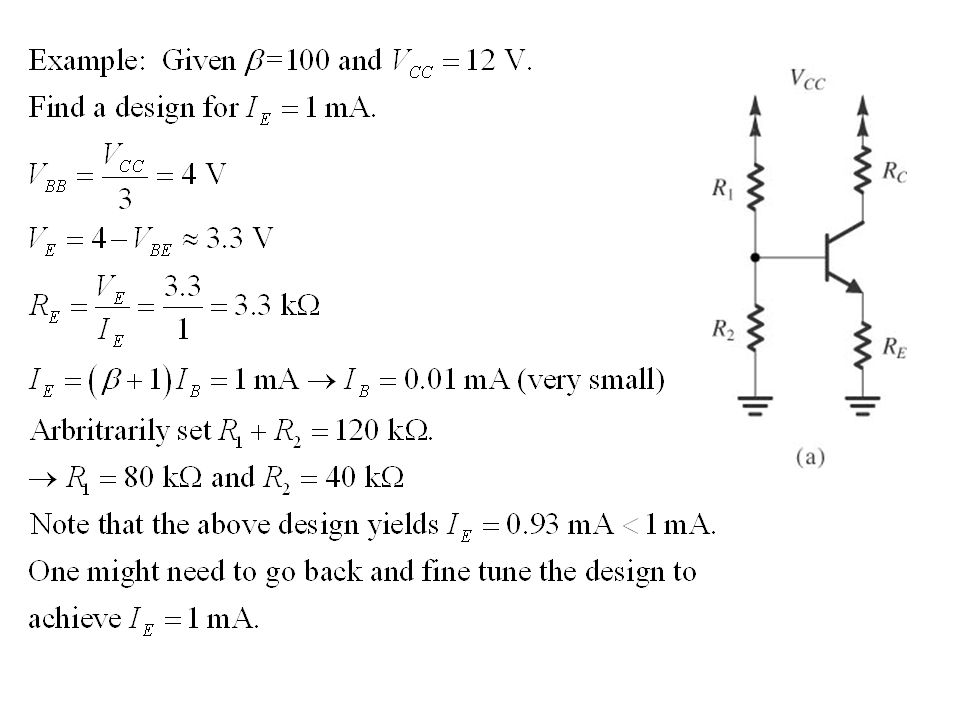
Input part + _ V BB _ + 10 V R B1 R B2 10 VR B2 V BB R B1 + _ V BB R BB

34
Biasing BJT Determining a quiescent point for linearization Active mode operation Considerations –Stable with respect to manufacturing parameters (e.g., r o, β) –Desired gains –Acceptable output swing
 –Desired gains –Acceptable output swing")
35
Biasing with Single Power Supply Fix V BE or I B. Output directly depends on β Unstable with respect to temperature variation

36
Addition of Degeneration Resistor

38
Biasing with Two Power Supplies

39
Biasing with Feedback Resistor

40
Biasing with Current Source

41
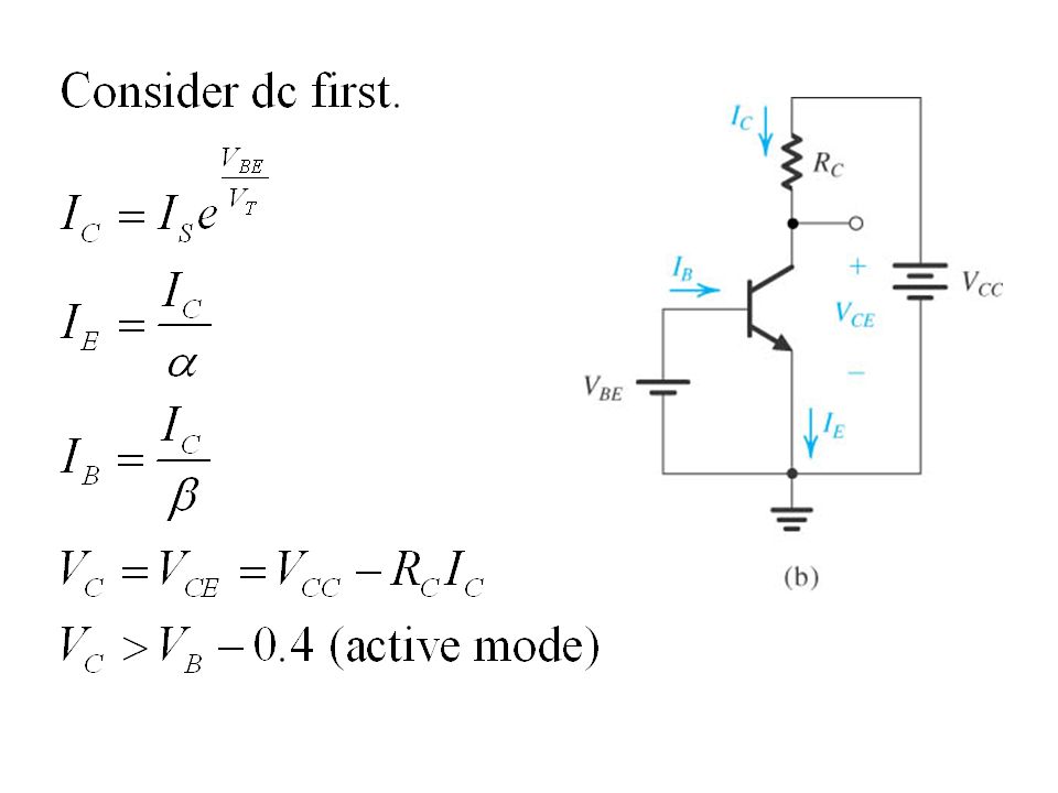
Small Signal Analysis A quiescent point has been determined by biasing. Active mode operation –Forward biasing for base-emitter junction by V BE –Reverse biasing for collector-base junction by R C and V CC

44
The transistor performs as a voltage controlled current source with gain g m when input varies by 10 mV or less.

48
Hybrid π Model Short circuit voltage sources Open circuit current sources Short circuit capacitors

50
T Model

54
Hybrid π Model with Early Effect

55
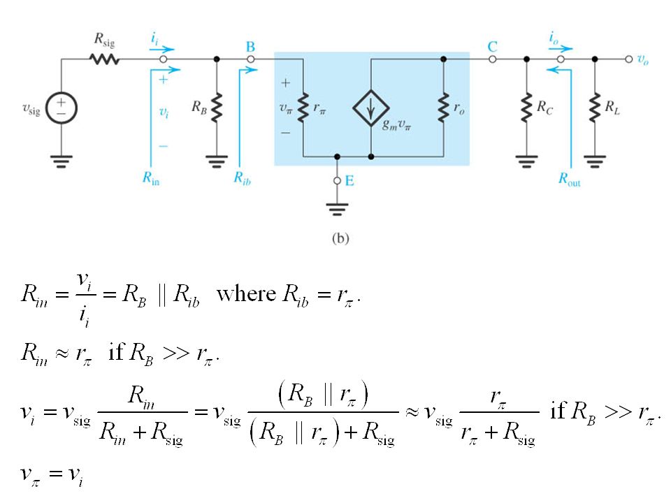
Structure of Single Stage Amplifier

56
Common Emitter Amplifier

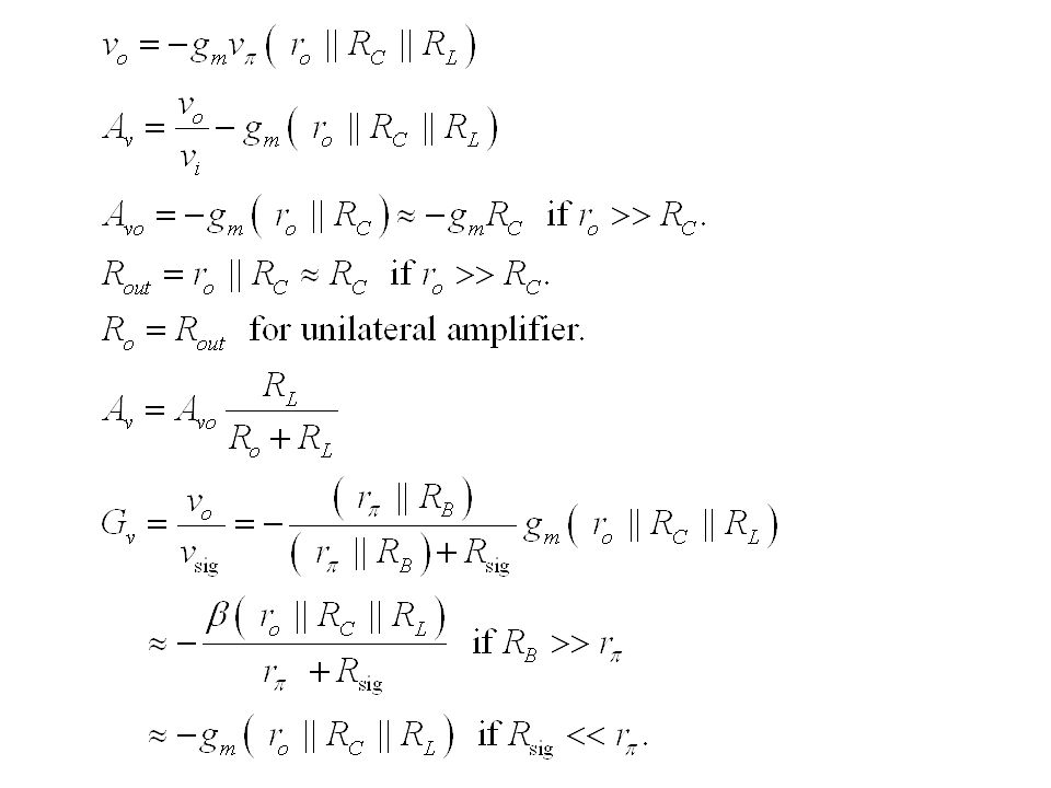
59
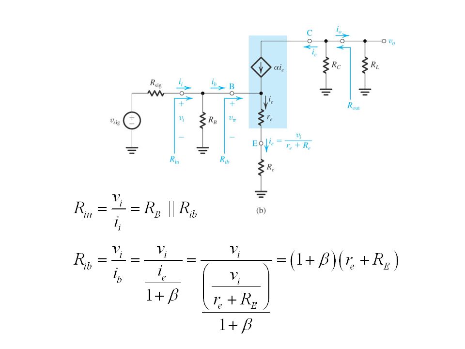
Common Emitter Amplifier with R E

62
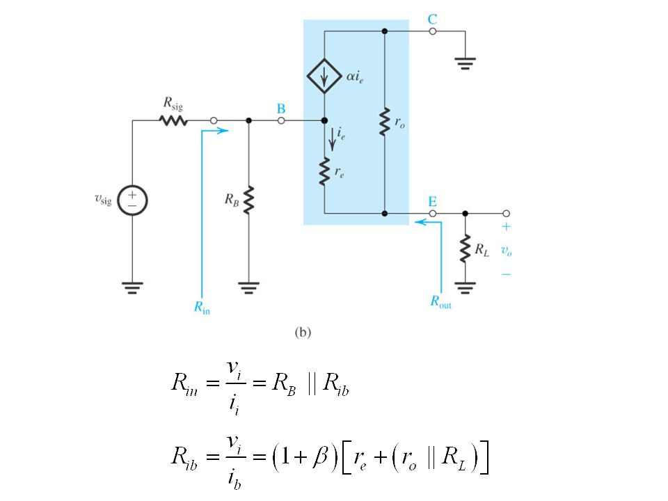
Common Base Amplifier

65
Common Collector Amplifier

69
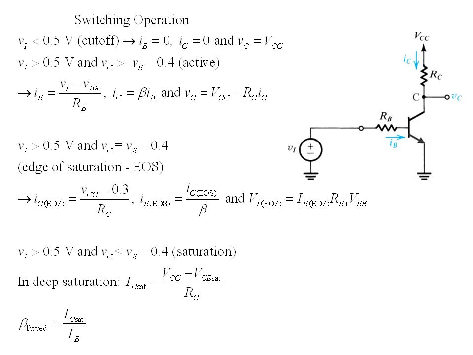
Digital Logic Inverter Transistor is in saturation mode. Logic 1: v I ≈ V CC → v O =V CEsat ≈ 0.2 V Logic 0: v I ≈ 0 → v O =V CC

70
v I – v O Transfer Function V CC = 5 V R B = 10 kΩ R C = 1 kΩ β = 50

Similar presentations


>")
 1.>")


 –3 layers of doped semiconductor –2 p-n junctions –Layers.>")

