Download presentation
Presentation is loading. Please wait.

1
Design Team 6 Alex Volinski Derek Brower Phil Jaworski Jung-Chung Lu Matt Affeldt

2
Software Flow Routing / Board Layout Components/Assembly Electrical Considerations

3
Software Packages Schematic Advantages Schematic creation ◦ Libraries ◦ ERC and simulation Schematic to Layout

4
Layout ◦ Libraries ◦ Layers and Routing ◦ Labels ◦ DRC Fabrication

5
Important Terminology ◦ Layers Metal Silkscreen Solder mask ◦ Traces ◦ Spaces ◦ Trace/Space

6
Important Terminology ◦ Pads Surface Mounts ◦ Vias Drilled Metal Plated Holes

7
Layout by importance of Position Align components in a common-sense approach Regulators Sensor IOSensor IO Sensor IOSensor IO Memory User I/O Micro- controller JTAG USB/ UART

8
Routing in PCB Artist ◦ Place components inside green PCB border ◦ Yellow lines are connections that need to be made

9
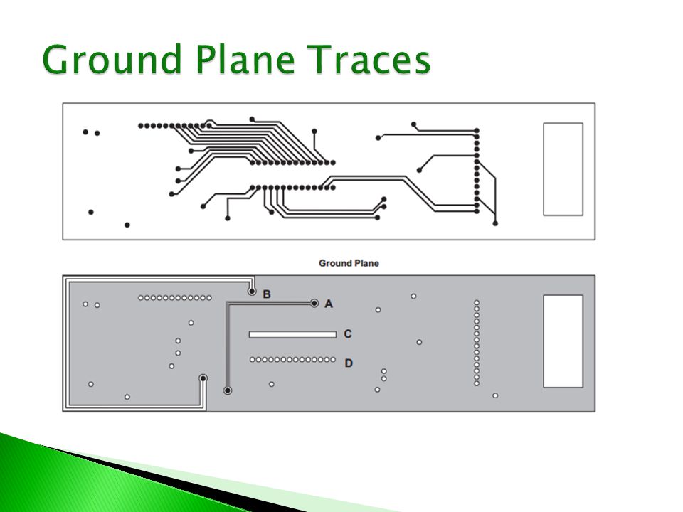
Layout Example of 2-Layer Board ◦ Bottom Level Grounded

10
Begin Making Traces

11
Tracing Problem

12
Grounding Techniques ◦ Series Common Impedance ◦ Parallel Low Potentials High Impedance ◦ Multipoint Contains Currents Reduces Inductance

13
Power Distribution ◦ Single-Point Single Reference ◦ Multipoint Impedance Coupled ◦ Star Distribution Central Reference Equal Lengths

14
Through-hole ◦ DIP Surface mount ◦ SOIC ◦ BGA ◦ QFN

15
Surface Mount ◦ Stay above 0805 Through Hole ◦ Much easier and less performance

16
Solder Reflow ◦ Allows precise soldering of Surface Mounts (below 0805)
")
17
Decreasing impedance vs. protecting a section

19
Multi-Layer board is capacitor

20
Avoiding Radiating EMI At ‘low’ frequencies (<100 MHz) no components will be antennas Be aware of attached cables Layout board to reduce coupling
 no components will be antennas Be aware of attached cables Layout board to reduce coupling")
21
Software Flow ◦ Advantage of making schematic ◦ Layers, Libraries, Fabrication Routing / Board Layout ◦ Layers, Traces, Pads vs. Vias ◦ Importance of position ◦ Grounding Techniques, Power Distribution

22
Components/Assembly ◦ Different types of components ◦ Through Hole / Surface Mount ◦ Weighing options for better performance Electrical considerations ◦ Stray Capacitance ◦ Ground Plane Traces ◦ Antennas to avoid radiating EMI

Similar presentations


 TA: Robert Likamwa ELEC 424, Fall 2010.>")


 design>")