Download presentation
Presentation is loading. Please wait.

1
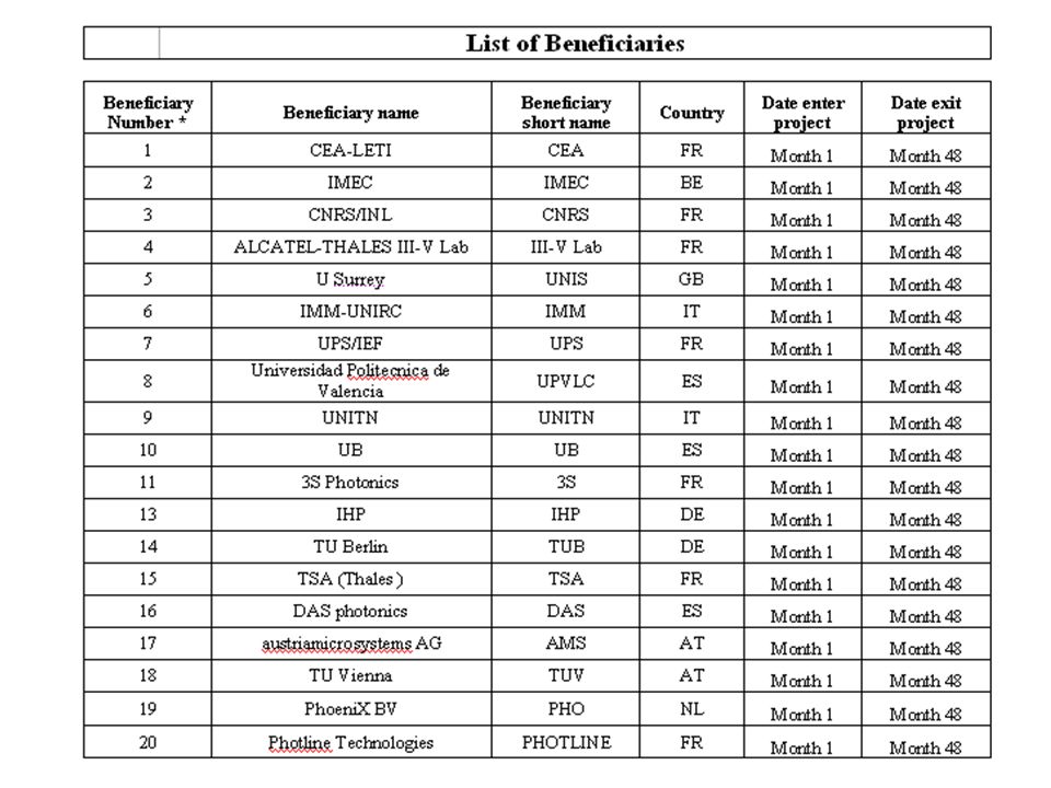
FP7-ICT-2007-2 HELIOS Large-scale Integrating Project Large-scale integrating project (IP) ICT Call 2 FP7-ICT-2007-2 pHotonics ELectronics functional Integration on CMOS HELIOS Date of preparation: 09.10.2007 Type of funding scheme: Large-scale integrating project (IP) Work programme topics addressed: ICT-2007.3.5: Photonic components and subsystems Name of the coordinating person: Laurent Fulbert e-mail: Laurent.fulbert@cea.fr Objectives: to build a complete design and fabrication chain enabling the integration of a photonic layer with a CMOS circuit, using microelectronics fabrication processes. It will make accessible integration technologies for a broad circle of users in a foundry-like, fabless way

2
–Demonstrating the power of this approach through demonstrators addressing different industrial needs –Preparing the future by exploring alternative approaches that offer clear advantages in terms of integration on CMOS. WP12: training and dissemination WP12: training and dissemination WP8: Modulator demonstrator WP8: Modulator demonstrator WP0 : Project management WP0 : Project management WP1: Roadmappingandexploitation WP1: Roadmappingandexploitation WP7: integration with CMOS WP2: source WP2: source WP3: modulator WP3: modulator WP4: passive circuitry WP4: passive circuitry WP5: photodetection WP5: photodetection WP6: packaging WP6: packaging WP9: Transceiver demonstrator WP9: Transceiver demonstrator WP11: innovative proof of concept WP11: innovative proof of concept WP10: PhotonicQAM Wireless transmission demonstrator WP10: PhotonicQAM Wireless transmission demonstrator photonics/electronics convergence at the process level and design level Different activities: –Developing the whole food chain high performance generic building blocks

4
Task 11.1 Amorphous Si modulator (IMM) Exploit amorphous silicon (a-Si:H) as a material to form a modulator to be fabricated at the end of the CMOS process. We plan to design, fabricate and characterise field-effect driven elements. The proposed basic technology is shown, with possible changes in the cladding layer. The proposed stacked modulator scheme highly enhances the electro-optical effects in the region where they are more effective on the propagating beam. WP11: INNOVATIVE PROOF OF CONCEPTS (CNRS)
.")
5
-Task 11.2: Silicon nanocrystals for light emission and amplification (UNITN) Realize an injection silicon laser based on active Er impurities which are excited via electrical injection into Si-nc embedded in a dielectric (oxide, nitride) 1. LED with Si-nc emitting at 0.75 μm with EQE of about 1% and a turn on voltage of less than 5V 2. LED with Er coupled to Si-nc emitting at 1.55 μm with same EQE and turn on voltage 3. Waveguide amplifiers with Er coupled to Si-nc, electrically driven and having a gain of 10 dB 4. Injection silicon laser emitting at 1.55 μm

6
Task 11.3 Novel concepts of heterogeneous integration (CNRS) This task will concentrate on the development of an innovative technological/conceptual scheme for 3D microphotonics on CMOS based on III-V/Silicon heterogeneous integration and diffractive photonics and opens the way to far larger functionality and wider potential impact than in the version of INTEL/PICMOS
 This task will concentrate on the development of an innovative technological/conceptual scheme for 3D microphotonics on CMOS based on III-V/Silicon heterogeneous integration and diffractive photonics and opens the way to far larger functionality and wider potential impact than in the version of INTEL/PICMOS")
7
IMM funding: Uni-RC IMM-BO IMM-Na RTD (A) [75%]: personnel, other direct costs [project specific materials needed for cleanroom, silicon substrates, process gases, chemicals, targets, consumables for polishing: 30k; parts needed for demonstrators (photomasks, fibers, glues): 5 k; travels: 10k] OTHER (D) [100%]: networking, organisation, dissemination (publications, participation to seminars, training) (indirect costs: 86,96% of personnel cost) Project duration: 48 months
![IMM funding: Uni-RC IMM-BO IMM-Na RTD (A) [75%]: personnel, other direct costs [project specific materials needed for cleanroom, silicon substrates, process gases, chemicals, targets, consumables for polishing: 30k; parts needed for demonstrators (photomasks, fibers, glues): 5 k; travels: 10k] OTHER (D) [100%]: networking, organisation, dissemination (publications, participation to seminars, training) (indirect costs: 86,96% of personnel cost) Project duration: 48 months](http://images.slideplayer.com/2/583763/slides/slide_7.jpg "IMM funding: Uni-RC IMM-BO IMM-Na RTD (A) [75%]: personnel, other direct costs [project specific materials needed for cleanroom, silicon substrates, process gases, chemicals, targets, consumables for polishing: 30k; parts needed for demonstrators (photomasks, fibers, glues): 5 k; travels: 10k] OTHER (D) [100%]: networking, organisation, dissemination (publications, participation to seminars, training) (indirect costs: 86,96% of personnel cost) Project duration: 48 months")
8
Tre strati Barriera: aSiCN 29 nm Cladding: nitruro simmetrico Barriera: aSiCN 30 nm Cladding: nitruro 1.5 micron 1 micron 3 strati Barriera: aSiCN 30 nm Cladding: nitruro Ultima barriera: aSiCN 1 micron 6 strati Barriera: aSiCN 38 nm Cladding: nitruro Ultima barriera: aSiCN 0.5 micron 6 strati SOTTILE: guide 0.2 micron, totale 1.2 micron Barriera: aSiCN 38 nm Cladding: nitruro Ultima barriera: aSiCN 0.2 micron 2 strati, ultra SOTTILE: guide 0.125 micron, totale 0.25 micron Barriera: aSiCN 40 nm Cladding: nitruro Ultima barriera: aSiCN 5 strati DROGATO: guide 0.25 micron, totale 1.25 micron Barriera: aSiC 40 nm Cladding: 1.1 micron SiO 2 Ultima barriera: SI Contatto ZnO 5 strati intrinseco in MDZ3: guide 0.25 micron, totale 1.25 micron Barriera: aSiC 40 nm Cladding: 1.1 micron SiO 2 Ultima barriera: SI Contatto ZnO ZnO c-Si tipo p c-Si tipo n ZnO c-Si tipo p c-Si tipo n

9
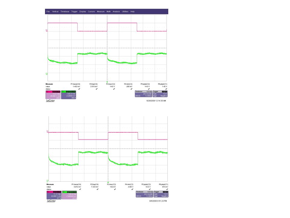
Segnale elettrico modulante Segnale ottico in uscita dalla guida

11
6 strati SOTTILE: guide 0.2 micron, totale 1.2 micron Barriera: aSiCN 38 nm Cladding: nitruro Ultima barriera: aSiCN 0.2 micron

13
ZnO

14
0.2 micron ITO

15
14167 a-Si:H 1.204 m SiO 2 R (%) 265 nm roughness 16211 A a-Si:H 663 A ITO2 3120 A SiO 2 R (%)
 265 nm roughness A a-Si:H 663 A ITO A SiO 2 R (%)")
16
0.2 micron ITO Spin-on-Glass

17
The following activities were performed study and optimisation of the films: a-Si:H, Si x N 1-x, a-SiC:H, a-SiCN films deposited and characterised, each in different stoichiometric compositions outcome: a-SiC:H will be used as insulator in future devices EXPERIMENTAL ACTIVITY electrical characterisationoptical characterisation

18
speed issues speed depends on =R C, where R resistivity of a-Si:H C doping has a key role log (time,s) log(electron, cm -3 ) simulated elec. conc. vs. time at the internal a-Si:H/insulator interfaces for different conductivities of a-Si:H t SiC (undoped)
.")
19
Drogaggio Aumenta la velocità Aumenta lassorbimento 80 sccm SiH 4 0.9 sccm PH 3 Ea = 0.16 eV D = 5.6 E-3 ( cm) -1 Simulazione nir: =30° K IR inferiore a 0.001
 -1 Simulazione nir: =30° K IR inferiore a 0.001")
20
V aumenta Red shift: aumenta nd Wavelength (nm) Misure ellissometro su modulatore polarizzato
 Misure ellissometro su modulatore polarizzato")
21
Meeting annuale: 16 giugno GRAZ

Similar presentations

>")

 with emphasis on.>")


: enhanced information retrieval and filtering for analytical systems Ying Ding.>")
>")


![1 M. Casalino [1][2], L. Sirleto [1], L. Moretti [2], I. Rendina [1] [1] Istituto per la Microelettronica e Microsistemi (IMM), Consiglio Nazionale delle.](/5/1594547/big_thumb.jpg "1 M. Casalino [1][2], L. Sirleto [1], L. Moretti [2], I. Rendina [1] [1] Istituto per la Microelettronica e Microsistemi (IMM), Consiglio Nazionale delle.>")


191 2087197.>")

