Download presentation
Presentation is loading. Please wait.

1
Example Computer Families Pentium 4 by Intel UltraSPARC III by Sun Microsystems The 8051 chip by Intel, used for embedded systems

2
Pentium 4 The Intel Corporation was formed in 1968. In 1970, Intel manufactured the first single- chip CPU, the 4-bit 4004 for a Japanese company to use in an electronic calculator. The 8088, a 16-bit CPU was chosen as the CPU for the original IBM PC. A series of backward compatible chips (80286, 386, 486, Pentium, Pentium Pro and Pentium II, III and 4) followed.
 followed..")
3
Intel Computer Family (1) The Intel CPU family. Clock speeds are measured in MHz (megahertz) where 1 MHZ is 1 million cycles/sec.
 where 1 MHZ is 1 million cycles/sec..")
4
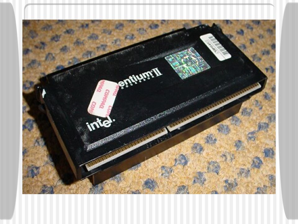
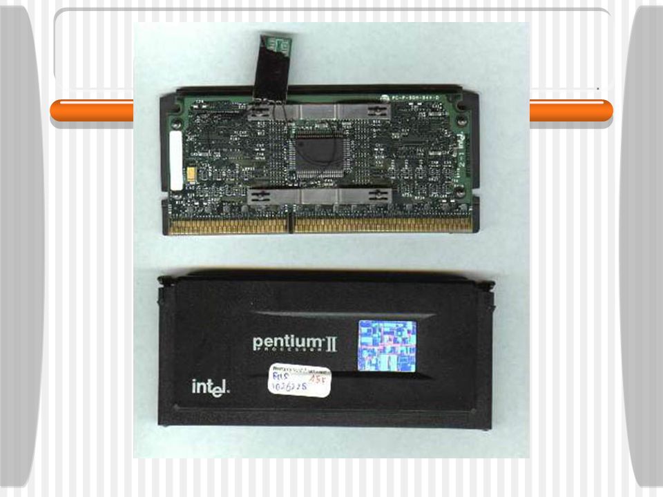
Intel Computer Family (2) The Pentium 4 chip. The photograph is copyrighted by the Intel Corporation, 2003 and is used by permission.

5
Intel Computer Family (3) Moore’s law for (Intel) CPU chips.
 Moore’s law for (Intel) CPU chips.")
6
Pentium 4

9
UltraSPARC III In the 1970s, UNIX was popular at universities, but it ran only on timeshared minicomputers such as the VAX and PDP-11 In 1981, a Stanford graduate student built a personal UNIX workstation using off-the-shelf parts. It was called the SUN-1. Early Sun workstations used Motorola CPUs. In 1987, Sun decided to design its own CPU based on a Cal Berkeley design called the RISC II.

10
UltraSPARC III The new CPU was called the SPARC (Scalable Processor ARChitecture) and was used in the Sun- 4. The SPARC was licensed to several semiconductor manufacturers who developed binary compatible versions. The first SPARC was a 32-bit machine with only 55 instructions (an FPU added 14 additional instructions). A 64-bit version, the UltraSPARC I was developed in 1995. This machine was aimed at high-end applications (e.g. web and database servers).
. A 64-bit version, the UltraSPARC I was developed in This machine was aimed at high-end applications (e.g. web and database servers)..")
13
MCS-51 Family The Intel 8051 is used in embedded systems Features 8-bit CPU Read only memory for the program RAM for variables 32 I/O lines 2 timers Serial port Low cost (10-15 cents per chip)
")
14
MCS-51 Family Members of the MCS-51 family.

15
The Pentium 4 It is fully backward compatible with the 8088 and can run unmodified 8088 binary programs. From a software point of view, the Pentium 4 is a full 32-bit machine. It has the same user-level ISA as the 80386, 80486, Pentium, Pentium Pro, Pentium II and III including the same registers, same instructions, and a full on- chip implementation of the IEEE 754 floating-point standard. From a hardware perspective, Pentium 4 is partially a 64-bit machine.

16
The Pentium 4 At the microarchitecture level, the Pentium II, III and Pentium Pro all used the P6 microarchitecture while Pentium 4 uses the NetBurst microarchitecture. Supports hyperthreading ISA level instructions are fetched from memory in advance and are broken up into RISC-like micro-operations stored in the L1 cache. All models have L2 cache, some have L3 as well.

17
The Pentium 4 The micro-operations are stored in a buffer, and as soon as one of them has the necessary resources to execute, it can be started. Multiple micro-operations can be started in the same cycle, making the Pentium 4 a superscalar machine. Snooping on the memory bus is supported so that multi-CPU systems can be built

18
The Pentium 4 Two primary external buses are used in Pentium 4 systems, both of them synchronous. The memory bus is used to address the main DRAM. The PCI bus is used for talking to I/O devices. Sometimes a legacy bus is attached to the PCI bus to allow the old peripheral devices to be plugged in.

19
The Pentium 4 The Pentium 4 physical pinout.

20
Pentium 4 478 Pins 85 power 180 ground Power consumption 63-82 watts Chip contains a mounting bracket for a heat sink

21
The Pentium 4’s Logical Pinout Logical pinout of the Pentium 4. Names in upper case are the office are the official Intel names for individual signals. Names in mixed case are groups of related signals or signal descriptions.

22
The Pentium 4 The Pentium 4 memory bus is pipelined with six stages: The bus arbitration phase The request phase The error reporting phase The snoop phase The response phase The data phase Not all phases are needed on all transactions. Each phase uses different bus signals.

23
The Pentium 4

24
The UltraSPARC III The UltraSPARC family is Sun’s line of 64-bit SPARC CPUs. It conforms to the Version 9 SPARC architecture. The UltraSPARC III is a traditional RISC machine and is fully binary compatible with the 32-bit SPARC V8 architecture. The UltraSPARC III was designed to build shared-memory multiprocessors without the need for external circuitry, and larger multiprocessors with minimal external circuitry.

25
The UltraSPARC III Unlike the Pentium II, the UltraSPARC III is a standalone chip (with 29 million transistors). It has 1369 pins on the bottom. The large number of pins is partly accounted for by the use of 64 bits for address and 128 bits for data, but also by the way caching works. The UltraSPARC III has two internal caches: 32 KB for data 64 KB for instructions It also has an off-chip level 2 cache

26
The UltraSPARC III The UltraSPARC III CPU chip.

27
The UltraSPARC III Most Sun workstations have a 25-MHz synchronous bus called the SBus. I/O devices can be plugged into the bus, but is too slow for memory. The UPA (Ultra Port Architecture) is a way for multiple UltraSPARC CPUs to communicate with multiple memories. It can be implemented as a bus, a switch, or a combination. The core of an UltraSPARC III system is shown on the following slide.
 is a way for multiple UltraSPARC CPUs to communicate with multiple memories. It can be implemented as a bus, a switch, or a combination. The core of an UltraSPARC III system is shown on the following slide..")
28
The UltraSPARC III

29
The UPA is implemented with a centralized controller. The address and control signals from the CPU go there. All incoming data goes to the UDB (UltraSPARC Data Buffer II), which buffers them. The purpose of the UDB is to decouple the memory system from the CPU so they can work asynchronously. The UDB also generates and checks the error- correcting code.
, which buffers them. The purpose of the UDB is to decouple the memory system from the CPU so they can work asynchronously. The UDB also generates and checks the error- correcting code..")
30
The 8051 Low cost Very popular Simple 40 pin package 16 address lines 8-bit wide data bus 32 I/O lines

31
The 8051 Physical pinout of the 8051.

32
The 8051 Logical pinout of the 8051.

33
The 8051 4 KB of internal ROM Can use up to 64 KB of external memory Note that many signals are multiplexed onto the same pins (save pins, reduce cost) The I/O lines can be connected directly to Button Switch LED etc.
 The I/O lines can be connected directly to Button Switch LED etc.")
34
The ISA Bus The IBM PC bus was the de facto standard on 8088-based systems because nearly all PC clone vendors copied it to allow existing third- party I/O boards to be used with their systems. It had 62 signal lines, including 20 for a memory address, 8 for data, and one each for asserting memory read, write, I/O read and write. The bus was etched onto the PCs motherboard with about half a dozen connectors for cards.

35
The ISA Bus

36
With the introduction of the 80286, IBM extended the PC bus. New cards had an extra edge connector at the bottom. With the introduction of the PS/2, IBM introduced a new bus, the Microchannel bus which was protected by patents. The rest of the industry reacted by adopting the ISA (Industry Standard Architecture) bus as a standard. This is basically a PC/AT bus running at 8.33 MHz.
 bus as a standard. This is basically a PC/AT bus running at 8.33 MHz..")
37
The PCI Bus With the introduction of GUIs, the ISA bus was no longer sufficiently powerful. In 1990, Intel designed a new bus with a much higher bandwidth than ISA or even EISA. It was called the PCI bus (Peripheral Component Interconnect bus). To encourage its use, Intel patented the PCI bus and then put all the patents into the public domain. Intel also formed an industry consortium to manage the future of the PCI bus.
. To encourage its use, Intel patented the PCI bus and then put all the patents into the public domain. Intel also formed an industry consortium to manage the future of the PCI bus..")
38
The PCI Bus As a result, the PCI bus has become extremely popular. The original PCI bus had a bandwidth of 133 MB/sec (32 bits per cycle and 33 MHz frequency - 30 nsec cycle time). PCI 2.2 runs at up to 528 MB/sec. In order to allow computers incorporating PCI buses to contain old peripherals, Intel designed computers with three or more buses. The buses are connected by bridge chips (manufactured by Intel).
. PCI 2.2 runs at up to 528 MB/sec. In order to allow computers incorporating PCI buses to contain old peripherals, Intel designed computers with three or more buses. The buses are connected by bridge chips (manufactured by Intel)..")
39
The PCI Bus

40
Pentium 4 Buses

41
The PCI Bus There are a variety of PCI card types: 5 or 3.3 volts 32-bit or 64-bit 33 MHz or 66 MHz The PCI bus is synchronous. All transactions are between a master and a slave. The address and data pins are multiplexed, thus only 64 pins are needed for address and data. The PCI bus uses a centralized bus arbiter. The arbiter is usually built into one of the bridge chips.

42
The PCI Bus

43
The algorithm used by the arbiter is not defined by the PCI specification. The PCI bus has a number of mandatory signals and a number of optional signals. The remainder of the 120 (32-bit version) or 184 pins (64-bit version) are used for power, ground, and related miscellaneous functions.
 or 184 pins (64-bit version) are used for power, ground, and related miscellaneous functions..")
44
PCI Express The new PCI Express architecture does away with the bus Replaced with a switch which has 2 unidirectional serial links to all I/O devices Devices send data packets to other devices Header of the packet contains control info An I/O device may actually be another switch The serial links are much smaller than PCI bus Devices are hot pluggable Error detection in the packets

45
PCI Express A typical PCI Express system.

46
The Universal Serial Bus The PCI bus is fine for attaching high-speed peripherals to a computer, but is far too expensive to have a PCI interface for each low- speed I/O device. Traditionally, new peripheral devices were inserted in free ISA and PCI slots. This can cause problems since the user is often responsible for setting switches and jumpers on the card and checking for conflicts with other cards. The user must open the case and insert the card then reboot the computer.

47
The Universal Serial Bus Representatives from seven companies designed a better way to attach low-speed I/O devices to a computer. The resulting standard is called USB (Universal Serial Bus). The goals of the project were: No jumpers or switches to set User doesn’t have to open the case Only one kind of cable I/O devices get power from the cable Up to 127 devices attachable to a single computer Real-time device support
. The goals of the project were: No jumpers or switches to set User doesn’t have to open the case Only one kind of cable I/O devices get power from the cable Up to 127 devices attachable to a single computer Real-time device support.")
48
The Universal Serial Bus Devices installable while the computer runs No reboot after installing a new device Inexpensive to manufacture USB meets these goals. The total USB 1.1 bandwidth is 1.5 MB/sec. A USB system consists of a root hub that plugs into the main bus. This hub has sockets for cables that attach to I/O devices. I/O devices also have sockets for additional devices. The topology of a USB system is a tree.

49
The Universal Serial Bus When a new I/O device is plugged in, the root hub detects the event and interrupts the OS. The OS then queries the device to find out what it is and how much bandwidth it needs. If the OS decides there is enough bandwidth available, it assigns the device a unique address (1-127) and downloads this address and other info to configuration registers inside the device.
 and downloads this address and other info to configuration registers inside the device..")
50
The Universal Serial Bus A USB system may be viewed as a set of bit pipes from the root hub to the I/O devices Within the pipes, data (frames) flow from the root hub to the I/O device or vice versa The root hub continuously broadcasts frames to keep the devices synchronized Frames consist of one or more packets
 flow from the root hub to the I/O device or vice versa The root hub continuously broadcasts frames to keep the devices synchronized Frames consist of one or more packets")
51
The Universal Serial Bus The USB root hub sends out frames every 1.00 ms.

52
USB 2.0 USB 2.0 is a newer faster version Bandwidth is 60 MB Backwards compatible with USB 1.1 devices Comparable speed to FireWire - a consumer electronics interface for digital camcorders, DVD players, etc.

Similar presentations


 2006 Pearson Education, Inc. All rights reserved. 0-13-148521-0 The Digital Logic Level.>")


 Buses Warning: some of the terminology is used inconsistently within the field.>")