Download presentation
Presentation is loading. Please wait.

1
Organic Optoelectronics Nir Tessler EE Dept. Microelectronic Center & Nanoelectronic Center Technion

2
The material: Organic semiconductors = molecular materials small molecules to long polymer chains. Length scale: Typical layer thickness – 50-100nm Inter chain distance ~ 0.5nm Semiconducting Organic Polymers Soluble Optoelectronic materials Nir Tessler, EE Dept., Technion

3
New Functional MaterialsNew/Improved Devices Chemically made Quantum Dots Semiconducting- polymer devices Chemical Synthesis Of semiconducting Molecules/polymers Biology Genetic engineering Uri BaninNir TesslerYoav EichenGad Schuster New Methods for Material Assembly Molecular Size Devices Libraries & precision In Polymer synthesis Macro- Devices New Functionalities “plastic” emitting at 1.3-1.5 m Nano Science and Technology Interdisciplinary Collaboration Chem. Dept Biology DeptEE Dept

4
New Functionalities Polymers emit visible light only! But optical communication elements operate with near infrared light can’t use polymers? OK – Lets mix ZnSe 0.99 1.26 CdSe InAs Shell 0.46 V E g 0.92 5 nm U.Banin, HebrewUniversity,Jerusalem Functional

5
Glass Ca\Al (cathode) PEDOT/ITO (Anode) n MeO O n O Polymer nanocrystal V - + Current/Energy is first injected into the polymer Energy/Charge Transfer to the nanocrystal Light Emission What do we hope to achieve by mixing
 PEDOT/ITO (Anode) n MeO O n O Polymer nanocrystal V - + Current/Energy is first injected into the polymer Energy/Charge Transfer to the nanocrystal Light Emission What do we hope to achieve by mixing")
6
Composite Emission in the NIR (>20V%NC) ~1% electroluminescence external efficiency. N. Tessler et. al., Science, 2002

7
Tessler et. al.,Science, 2002 Plastics for telecomm The potential Impact

8
We are not yet capable to accurately predict the optoelectronic properties associated with a given chemical structure A Known Solution: Make many structures (libraries) Screen and cross correlate properties structure A TIP: In biology, Peptide synthesis, is a fully developed automatic method. Libraries

9
Libraries of -Conjugated Polymers from Fiction to Science?

10
Solid State Peptide Synthesis First Attempt S. Tal, Y. Eichen will the material remain a semiconductor when such unit is used as a linker?

11
Peptide synthesis valid for conjugated molecules/polymers Gate voltage dependence IDID ISIS VGVG Peptide SiO 2 Au Field Effect Transistor =0 V G > 0

12
What Do we (in EE) contribute to this material/chemistry dominated field? Investigate the internal processes. Learn how the material property affect the device performance. Know how to extract the material properties as manifested in a working device. Provide feedback to materials/chemistry

13
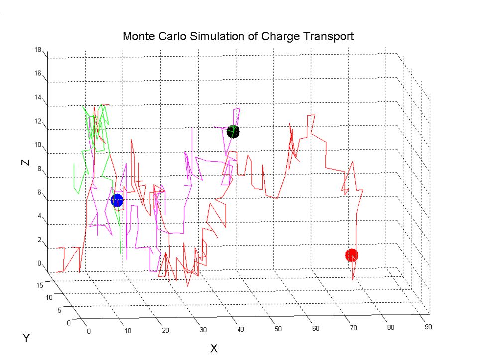
Level 1 The material is made of discrete molecules. Charge is hopping between sites that are distributed in space and energy. Charge Transport Monte-Carlo Simulation Gaussian Density of States (width ) E Y. Bar
 E Y. Bar.")
15
What do we extract from it? Can we apply statistics to describe the motion. Can we use Fermi-Dirac Statistics? Can we define a quasi-equilibrium? Can we use the notion of: mobility ( ) diffusivity (D) If yes we can use/create device models
 diffusivity (D) If yes we can use/create device models.")
16
Assume: 1. Yes, we can use D and 2. Energy distribution of sites- Gaussian What value/function ( E,n) should we use in a device model?
 should we use in a device model .")
17
Ratio Between D and (Einstein relation) The semiconductor is degenerate for (almost) every practical density Built-in charge density dependence of the transport phenomena LED device FET device Y. Roichman

18
Use the Physical picture to study A very practical problem HOMO Level (Valence “band”) LUMO Level (Conduction) Metal Energy EE Standard text book Model :
 LUMO Level (Conduction) Metal Energy EE Standard text book Model :")
19
Device Model of a contact region 3-10nm Y. Preezant

20
The contact as simulated within a DEVICE model Introducing the effect of the Einstein Relation Only =4kT =2kT <<kT Using text book analysis: E is temperature dependent 2.Contact phenomena is unpredictable Using the NEW model: 1.Good Agreement between Theory and Experiment 2.Contact phenomena is predictable (As was shown on the poster)
")
21
The contact phenomena (Through 2D modeling of Field Effect Transistor) polymer Charge Density (10 18 cm -3 ) Insulator Length ( m) Depth ( m) Drain Source S’ D’ t= t D’S’
 polymer Charge Density (10 18 cm -3 ) Insulator Length ( m) Depth ( m) Drain Source S’ D’ t= t D’S’")
22
Charge Density (10 18 cm -3 ) Length ( m) Depth ( m) polymer Insulator Drain Source Channel Charge at steady state V S = 0V V D = -3V V G = -5V D’ S’ Track the charges, Potential drops (associated with the structure), …. Know how to translate Device performance to Material Performance Close the loop with the Material/Chemistry part

23
Chemistry/Materials Device Modeling Device Design & measure Analysis and extraction of properties New FunctionalitiesNovel Materials

24
Thanks To Yoav Eichen Shay Tal Uri Banin Miri Kazes Shi-hi Kan Vlad Medvedev Yevgeni Preezant Yhoram Bar Yohai Roichman Noam Rapaport Olga Solomeshch Alexey Razin Yair Ganot Sagi Shaked Avecia Chemicals Israel Science Foundation European Union FW-6 $

Similar presentations


 2013/10/30.>")


 whereas.>")


 授課老師:林寬鋸 教授 http://web.nchu.edu.tw/pweb/users/kjlin.>")


 Prof.>")