Download presentation
Presentation is loading. Please wait.

1
AMPLIFIERS, DIODES,RECTIFIERS,WAVESHAPPING CIRCUITS
AMPLIFIERS: Ideal op-amp and Practical op-amp DIODES RECTIFIERS: half wave, full wave WAVESHAPPING CIRCUITS : clippers, clampers

2
AMPLIFIERS: Ideal op-amp and Practical op-amp
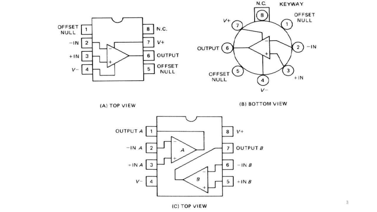
Operational Amplifiers are represented both schematically and realistically below: An operational amplifier, or op-amp, is a very high gain differential amplifier with high input impedance and low output impedance

4
3-stage Op-Amp

5
Attenuates and phases at high frequencies (depends on slew rate)
Ideal Op Amp Zin is infinite; Zout is zero; Amplification (Gain) Vout / Vin = ∞; Unlimited bandwidth; Vout = 0 when Voltage inputs = 0 Ideal Op-Amp Typical Op-Amp Input Resistance infinity 106 (bipolar) 109 (FET) Input Current 10-12 – 10-8 A Output Resistance 100 – 1000 Operational Gain Common Mode Gain 10-5 Bandwidth Attenuates and phases at high frequencies (depends on slew rate) Temperature independent Bandwidth and gain
 Vout / Vin = ∞; Unlimited bandwidth; Vout = 0 when Voltage inputs = 0. Ideal Op-Amp. Typical Op-Amp. Input Resistance. infinity. 106 (bipolar) 109 (FET) Input Current – 10-8 A. Output Resistance. 100 – 1000 Operational Gain Common Mode Gain Bandwidth. Attenuates and phases at high frequencies (depends on slew rate) Temperature. independent. Bandwidth and gain.")
6
Single-Ended Input

7
Double-Ended (Differential) Input
 Input")
8
Double-Ended Output

9
Common-Mode Operation Common-Mode Rejection
The signals which are opposite at the inputs are highly amplified, while those which are common to the two inputs are only slightly amplified—the overall operation is to amplify the difference signal while rejecting the common signal at the two inputs. Noise (any unwanted input signal) is generally common to both inputs, the differential connection tends to provide attenuation of this unwanted input while providing an amplified output of the difference signal applied to the inputs.
 is generally common to both inputs, the differential connection tends to provide attenuation of this unwanted input while providing an amplified output of the difference signal applied to the inputs.")
10
Differential Inputs Common Inputs Output Voltage where Vd difference voltage Vc common voltage Ad differential gain of the amplifier Ac common-mode gain of the amplifier

11
Same Polarity Inputs Opposite Polarity Inputs
If opposite polarity inputs applied to an op-amp are ideally opposite signals, Vi1= -Vi2 =Vs, the resulting difference voltage is The resulting common voltage is The resulting output voltage is Same Polarity Inputs If the same polarity inputs are applied to an op-amp, , the resulting difference voltage is

12
The resulting common voltage is
The resulting output voltage is Common-Mode Rejection Ratio The value of CMRR can also be expressed in logarithmic terms

13
EXAMPLE Calculate the CMRR for the circuit measurements

14
Inverting Op-Amp Non-inverting Op-Amp

15
Summation Difference If all resistors are equal:

16
Differentiating Op-Amp
Integrating Op-Amp Differentiating Op-Amp (where Vin and Vout are functions of time)
")
17
SEMICONDUCTOR Si Cu*1011 · cm , Ge Cu*107 · cm
Intrinsic (pure) Semiconductors Different types of solids: Conductor < 10-4 ·cm Insulator 1010 · cm Semiconductor Si Cu*1011 · cm , Ge Cu*107 · cm The atomic structure of a neutral silicon atom Valence electrons
 Semiconductors. Different types of solids: Conductor < 10-4 ·cm. Insulator 1010 · cm. Semiconductor Si Cu*1011 · cm , Ge Cu*107 · cm. The atomic structure of a neutral silicon atom. Valence electrons.")
18
Intrinsic (pure) Semiconductors
A hole Intrinsic(pure) silicon A free electron An electron-hole pair is created when an electron get excited by thermal or light energy; Recombination occurs when an electron loses energy and falls back into a hole.
 silicon. A free electron. An electron-hole pair is created when an electron get excited by thermal or light energy; Recombination occurs when an electron loses energy and falls back into a hole.")
19
Intrinsic (pure) Semiconductors
Holes also conduct current. In reality, it’s the movement of all the other electrons. The hole allows this motion. Holes have positive charge. • Current flows in the same direction as the holes move. Both electrons and holes carry current-- carriers. In intrinsic semiconductors the electron and hole concentrations are equal because carriers are created in pairs The intrinsic concentration depends exponentially on temperature. At room temp (300K), the intrinsic carrier concentration of silicon is:
, the intrinsic carrier concentration of silicon is:")
20
Phosphorus Doping (N-type)
Phosphorus has 5 valence electrons. • P atoms will sit in the location of a Si atom in the lattice, to avoid breaking symmetry, but each will have an extra electron that does not bond in the same way. And these extra electrons are easier to excite (and can move around more easily) • These electrons depends on the amounts of the two materials.
 • These electrons depends on the amounts of the two materials.")
21
Phosphorus Doping (N-type)
Electrons---Majority carrier. Holes---Minority carrier Phosphorus---Donor materials. In equilibrium, At room temp (300K), if 1/1010 donors are added to the intrinsic silicon, then the electron carrier concentration is about 1013cm-3; the hole carrier concentration is about 106cm-3. Phosphorus Intrinsic silicon
, if 1/1010 donors are added to the intrinsic silicon, then the electron carrier concentration is about 1013cm-3; the hole carrier concentration is about 106cm-3. Phosphorus Intrinsic silicon.")
22
Boron---acceptor materials.
Boron Doping (P-type) Holes---Majority carrier; Electrons---Minority carrier Boron---acceptor materials. Boron has 3 valence electrons. • B will sit at a lattice site, but the adjacent Si atoms lack an electron to fill its shell. This creates a hole.
 Holes---Majority carrier; Electrons---Minority carrier. Boron---acceptor materials. Boron has 3 valence electrons. • B will sit at a lattice site, but the adjacent Si atoms lack an electron to fill its shell. This creates a hole.")
23
PN Junction N-type materials: Doping Si with a Group V element, providing extra electrons (n for negative) . P-type materials: Doping Si with a Group III element, providing extra holes (p for positive). What happens when P-type meets N-type?
. What happens when P-type meets N-type")
24
PN Junction What happens when P-type meets N-type?
Holes diffuse from the P-type into the N-type, electrons diffuse from the N-type into the P-type, creating a diffusion current. • Once the holes [electrons] cross into the N-type [P-type] region, they recombine with the electrons [holes]. • This recombination “strips” the n-type [P-type] of its electrons near the boundary, creating an electric field due to the positive and negative bound charges. • The region “stripped” of carriers is called the space-charge region, or depletion region. • V0 is the contact potential that exists due to the electric field. Typically, at room temp, V0 is 0.5~0.8V. • Some carriers are generated (thermally) and make their way into the depletion region where they are whisked away by the electric field, creating a drift current.
 and make their way into the depletion region where they are whisked away by the electric field, creating a drift current.")
25
PN Junction – Drift What happens when P-type meets N-type?
There are two mechanisms by which mobile carriers move in semiconductors – resulting in current flow – Diffusion • Majority carriers move (diffuse) from a place of higher concentration to a place of lower concentration – Drift • Minority carrier movement is induced by the electric field. In equilibrium, diffusion current (ID) is balanced by drift current (IS). So, there is no net current flow.
 from a place of higher. concentration to a place of lower concentration. – Drift. • Minority carrier movement is induced by the electric field. In equilibrium, diffusion current (ID) is balanced by drift current (IS). So, there is no net current flow.")
26
PN Junction Forward bias: apply a positive voltage to the P-type, negative to N-type. Add more majority carriers to both sides shrink the depletion region lower V0 diffusion current increases. Decrease the built-in potential, lower the barrier height. • Increase the number of carriers able to diffuse across the barrier • Diffusion current increases • Drift current remains the same. The drift current is essentially constant, as it is dependent on temperature. • Current flows from p to n

27
PN Junction Reverse bias: apply a negative voltage to the P-type, positive to N-type. Increase the built-in potential, increase the barrier height. • Decrease the number of carriers able to diffuse across the barrier. • Diffusion current decreases. • Drift current remains the same • Almost no current flows. Reverse leakage current, IS, is the drift current, flowing from N to P.

28
PN Junction Diode V-A Characteristic
In forward bias, the PN junction has a “turn on” voltage based on the “built-in” potential of the PN junction. turn on voltage is typically in the range of 0.5V to 0.8V In reverse bias, the PN junction conducts essentially no current until a critical breakdown voltage is reached. The breakdown voltage can range from 1V to 100V. Breakdown mechanisms include avalanche and zener tunneling. PN Junction Diode V-A Characteristic

29
PN Junction Diode V-A Characteristic
Current Equations • The forward bias current is closely approximated by where VT =kT/q is the thermal voltage (~25.8mV at room temp T= 300K or 27C ) k = Boltzman’s constant = 1.38 x joules/kelvin T = absolute temperature q = electron charge = x coulombs n = constant dependent on structure, between 1 and 2 (we will assume n = 1) IS = scaled current for saturation current that is set by diode size – There is a strong dependence on temperature – We can approximate the diode equation for vD >> VT ,
 k = Boltzman’s constant = 1.38 x joules/kelvin. T = absolute temperature. q = electron charge = x coulombs. n = constant dependent on structure, between 1 and 2 (we will assume n = 1) IS = scaled current for saturation current that is set by diode size. – There is a strong dependence on temperature. – We can approximate the diode equation for vD >> VT ,")
30
• In reverse bias (when vD << 0 by at least VT ), then
• In breakdown, reverse current increases rapidly… a vertical line Example: PN Junction when T = 300K, Find iD when

31
Diode Models-- The Ideal Switch Model
When forward-biased, the diode ideally acts as a closed (on) witch. When reverse-biased, the diode acts as an open (off) switch.
 witch. When reverse-biased, the diode acts as an open (off) switch.")
32
Diodes

Similar presentations


>")


