Download presentation
Presentation is loading. Please wait.

1
DPSD This PPT Credits to : Ms. Elakya - AP / ECE.
NOTE : This PPT has not been Completed. Will be updated shortly.. Best viewed in : MS-Office 2013 / Premium! Customized by : IT Rockz!

2
COMBINATIONAL CIRCUITS

3
ANALYSIS PROCEDURE To obtain the output Boolean functions from a logic diagram, proceed as follows: 1. Label all gate outputs that are a function of input variables with arbitrary symbols.Determine the Boolean functions for each gate output. 2. Label the gates that are a function of input variables and previously labeled gates with other arbitrary symbols. Find the Boolean functions for these gates.

4
3. Repeat the process outlined in step 2 until the outputs of the circuit are obtained.
4. By repeated substitution of previously defined functions, obtain the output Boolean functions in terms of input variables.

5
DESIGN PROCEDURE Step 1: Analyze the given problem
Step 2:Determine the number of input and output variables. Step 3:Assigning letter symbols to input and output Step 4:Derive the truth table indicating the relationships between input and output variables. Step 5:Obtain the simplified boolean functions for each output variable by using K-map. Step 6:Draw the logic diagram for the above simplified expression by using logic gates.

6
Block Diagram of Half Adder
A logic circuit which performs the arithmetic addition of two bits is called a half adder. The circuit that will add two input bits (augend and addend) and produce a two binary output: sum and a carry bit. Block Diagram of Half Adder
 and produce a two binary output: sum and a carry bit. Block Diagram of Half Adder.")
7
TRUTH TABLE

8
K - MAP

9
LOGIC DIAGRAM OF HALF ADDER

10
FULL ADDER A full adder is a combinational logic circuits that performs the arithmetic sum of three inputs bits. Full adder Circuit will add three bits and produce two outputs a sum and a carry bits. The third input Cin represents the carry from the previous lower significant position Block Diagram of Full Adder

11
TRUTH TABLE

12
K- Map

13
LOGIC DIAGRAM OF FULL ADDER

14
FULL ADDER USING TWO HALF ADDER AND OR GATE

15
HALF SUBTRACTOR Half Subtractor is a combinational logic circuit that subtracts two bits and produced their difference and borrow The half subtractor needs two inputs:minuend and subtrahend bits and two output bits : borrow and difference. Block Diagram of Half Subtractor

16
TRUTH TABLE

17
K-Map

18
LOGIC DIAGRAM

19
FULL SUBTRACTOR Block Diagram of full subtractor
A full subtractor is a combinational logic circuit that performs subtraction involving three bits, namely minuend bit, subtrahend bit and the borrow from the previous stage. Block Diagram of full subtractor

20
TRUTH TABLE

21
K-Map

22
LOGIC DIAGRAM

23
FULL SUBTRACTOR USING TWO HALF SUBTRACTOR AND OR GATE

24
BINARY ADDER

25
BINARY ADDER Binary adder that produces the arithmetic sum of binary numbers can be constructed with full adders connected in cascade, with the output carry from each full adder connected to the input carry of the next full adder in the chain Note that the input carry C0 in the least significant position must be 0.

26
4 BIT BINARY ADDER

27
BINARY SUBTRACTOR

28
BINARY SUBTRACTOR The subtrcation A – B can be done by taking the 2’s complement of B and adding it to A because A- B = A + (-B) It means if we use the inveters to make 1’s complement of B (connecting each Bi to an inverter) and then add 1 to the least significant bit (by setting carry C0 to 1) of binary adder, then we can make a binary subtractor
 and then add 1 to the least significant bit (by setting carry C0 to 1) of binary adder, then we can make a binary subtractor.")
29
BINARY ADDER/SUBTRACTOR

30
BINARY ADDER/SUBTRACTOR
The addition and subtraction can be combined into one circuit with one common binary adder. The mode M controls the operation. When M=0 the circuit is an adder when M=1 the circuit is subtractor. It can be don by using exclusive-OR for each Bi and M. Note that 1 ⊕ x = x’ and 0 ⊕ x = x

31
CARRY LOOK AHEAD ADDER Most other arithmetic operations, e.g. multiplication and division are implemented using several add/subtract steps. Thus, improving the speed of addition will improve the speed of all other arithmetic operations. Accordingly, reducing the carry propagation delay of adders is of great importance. Different logic design approaches have been employed to overcome the carry propagation problem.

32
One widely used approach employs the principle of carry look-ahead solves this problem by calculating the carry signals in advance, based on the input signals. This type of adder circuit is called as carry look-ahead adder (CLA adder). It is based on the fact that a carry signal will be generated in two cases: (1) when both bits Ai and Bi are 1, or (2) when one of the two bits is 1 and the carry-in (carry of the previous stage) is 1.
. It is based on the fact that a carry signal will be generated in two cases: (1) when both bits Ai and Bi are 1, or. (2) when one of the two bits is 1 and the carry-in (carry of the previous stage) is 1.")
33
The Figure shows the full adder circuit used to add the operand bits in the ith column; namely Ai & Bi and the carry bit coming from the previous column (Ci ).
.")
35
The Boolean expression of the carry outputs of various stages can be written as follows:
C1 = G0 + P0C0 C2 = G1 + P1C1 = G1 + P1 (G0 + P0C0) = G1 + P1G0 + P1P0C0 C3 = G2 + P2C2 = G2 + P2G1 + P2P1G0 + P2P1P0C0 C4 = G3 + P3C3 = G3 + P3G2 + P3P2G1 + P3P2P1G0 + P3P2P1P0C0
 = G1 + P1G0 + P1P0C0. C3 = G2 + P2C2 = G2 + P2G1 + P2P1G0 + P2P1P0C0. C4 = G3 + P3C3. = G3 + P3G2 + P3P2G1 + P3P2P1G0 + P3P2P1P0C0.")
36
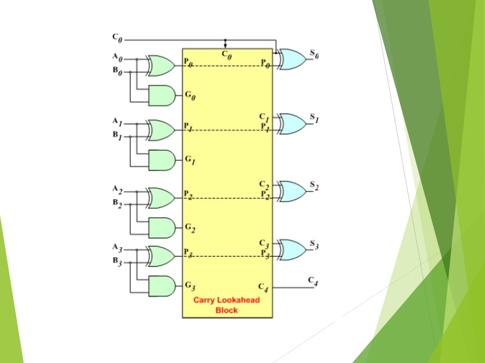
Logic Diagram of a look ahead carry generator

38
BCD ADDER

39
BLOCK DIAGRAM OF BCD ADDER

40
BINARY MULTIPLIER

Similar presentations


>")
 Lecture-8:>")


 Chapter 4 – Arithmetic Functions Logic and Computer.>")


