Download presentation
Presentation is loading. Please wait.

1
Combinational Circuits

3
Designing Combinational Circuits
In general we have to do following steps: Problem description Input/output of the circuit Define truth table Simplification for each output Draw the circuit

8
Binary adder Binary adder that produces the arithmetic sum of binary numbers can be constructed with full adders connected in cascade, with the output carry from each full adder connected to the input carry of the next full adder in the chain Note that the input carry C0 in the least significant position must be 0.

9
Binary Adder

10
Binary Adder For example to add A= 1011 and B= 0011
subscript i: Input carry: Ci Augend: Ai Addend: Bi Sum: Si Output carry: Ci+1

11
Binary Subtractor The subtrcation A – B can be done by taking the 2’s complement of B and adding it to A because A- B = A + (-B) It means if we use the inveters to make 1’s complement of B (connecting each Bi to an inverter) and then add 1 to the least significant bit (by setting carry C0 to 1) of binary adder, then we can make a binary subtractor.
 and then add 1 to the least significant bit (by setting carry C0 to 1) of binary adder, then we can make a binary subtractor.")
12
4 bit 2’s complement Subtractor
= 1

13
Adder Subtractor The addition and subtraction can be combined into one circuit with one common binary adder (see next slide). The mode M controls the operation. When M=0 the circuit is an adder when M=1 the circuit is subtractor. It can be don by using exclusive-OR for each Bi and M. Note that 1 ⊕ x = x’ and 0 ⊕ x = x

15
Checking Overflow Note that in the previous slide if the numbers considered to be signed V detects overflow. V=0 means no overflow and V=1 means the result is wrong because of overflow Overflow can be happened when adding two numbers of the same sign (both negative or positive) and result can not be shown with the available bits. It can be detected by observing the carry into sign bit and carry out of sign bit position. If these two carries are not equal an overflow occurred. That is why these two carries are applied to exclusive-OR gate to generate V.
 and result can not be shown with the available bits. It can be detected by observing the carry into sign bit and carry out of sign bit position. If these two carries are not equal an overflow occurred. That is why these two carries are applied to exclusive-OR gate to generate V.")
16
Magnitude Comparator It is a combinational circuit that compares to numbers and determines their relative magnitude The output of comparator is usually 3 binary variables indicating: A>B A=B A<B For example to design a comparator for 2 bit binary numbers A (A1A0) and B (B1B0) we do the following steps:
 and B (B1B0) we do the following steps:")
17
Comparators For a 2-bit comparator we have four inputs A1A0 and B1B0 and three output E ( is 1 if two numbers are equal) G (is 1 when A > B) and L (is 1 when A < B) If we use truth table and KMAP the result is E= A’1A’0B’1B’0 + A’1A0B’1B0 + A1A0B1B0 + A1A’0B1B’0 or E=(( A0 ⊕ B0) + ( A1 ⊕ B1))’ (see next slide) G = A1B’1 + A0B’1B’0 + A1A0B’0 L= A’1B1 + A’1A’0B0 + A’0B1B0 A0 Comparator E A1 G B0 L B1
 G (is 1 when A > B) and L (is 1 when A < B) If we use truth table and KMAP the result is. E= A’1A’0B’1B’0 + A’1A0B’1B0 + A1A0B1B0 + A1A’0B1B’0. or E=(( A0 ⊕ B0) + ( A1 ⊕ B1))’ (see next slide) G = A1B’1 + A0B’1B’0 + A1A0B’0. L= A’1B1 + A’1A’0B0 + A’0B1B0. A0. Comparator. E. A1. G. B0. L. B1.")
18
Magnitude Comparator Here we use simpler method to find E (called X) and G (called Y) and L (called Z) A=B if all Ai= Bi Ai Bi Xi It means X0 = A0B0 + A’0B’0 and X1= A1B1 + A’1B’1 If X0=1 and X1=1 then A0=B0 and A1=B1 Thus, if A=B then X0X1 = 1 it means X= (A0B0 + A’0B’0)(A1B1 + A’1B’1) since (x ⊕ y)’ = (xy +x’y’) X= ( A0 ⊕ B0)’ ( A1 ⊕ B1)’ = (( A0 ⊕ B0) + ( A1 ⊕ B1))’ It means for X we can NOR the result of two exclusive-OR gates
(A1B1 + A’1B’1) since (x ⊕ y)’ = (xy +x’y’) X= ( A0 ⊕ B0)’ ( A1 ⊕ B1)’ = (( A0 ⊕ B0) + ( A1 ⊕ B1))’ It means for X we can NOR the result of two exclusive-OR gates.")
19
Magnitude Comparator A>B means A1 B1 Y1 ------------ 0 0 0 0 1 0
if A1=B1 (X1=1) then A0 should be 1 and B0 should be 0 A0 B0 Y0 For A> B: A1 > B1 or A1 =B1 and A0 > B0 It means Y= A1B’1 + X1A0B’0 should be 1 for A>B
 then A0 should be 1 and B0 should be 0. A0 B0 Y For A> B: A1 > B1 or A1 =B1 and A0 > B0. It means Y= A1B’1 + X1A0B’0 should be 1 for A>B.")
20
Magnitude Comparator For B>A B1 > A1 or A1=B1 and B0> A0
z= A’1B1 + X1A’0B0 The procedure for binary numbers with more than 2 bits can also be found in the similar way. For example next slide shows the 4-bit magnitude comparator, in which (A= B) = x3x2x1x0 (A> B) = A3B’3 + x3A2B’2 + x3x2A1B’1+ x3x2x1A0B’0 (A< B) = A’3B3 + x3A’2B2 + x3x2A’1B1+ x3x2x1A’0B0
 = x3x2x1x0. (A> B) = A3B’3 + x3A2B’2 + x3x2A1B’1+ x3x2x1A0B’0. (A< B) = A’3B3 + x3A’2B2 + x3x2A’1B1+ x3x2x1A’0B0.")
22
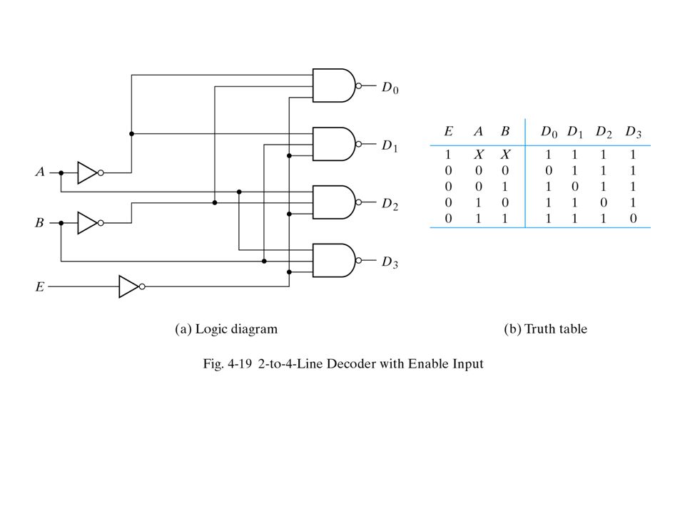
Decoder Is a combinational circuit that converts binary information from n input lines to a maximum of 2n unique output lines For example if the number of input is n=3 the number of output lines can be m=23 . It is also known as 1 of 8 because one output line is selected out of 8 available lines: 3 to 8 decoder enable

24
Decoder with Enable Line
Decoders usually have an enable line, If enable=0 , decoder is off. It means all output lines are zero If enable=1, decoder is on and depending on input, the corresponding output line is 1, all other lines are 0 See the truth table in next slide

25
Truth table for decoder
E a2 a1 a0 D7 D6 D5 D4 D3 D2 D1 D0 0 x x x 1 ………………………………………. ……………………………………..

27
Major application of Decoder
Decoder is use to implement any combinational cicuits ( fn ) For example the truth table for full adder is s (x,y,z) = ∑ ( 1,2,4,7) and C(x,y,z)= ∑ (3,5,6,7). The implementation with decoder is:
 For example the truth table for full adder is s (x,y,z) = ∑ ( 1,2,4,7) and C(x,y,z)= ∑ (3,5,6,7). The implementation with decoder is:")
28
Encoder Encoder is a digital circuit that performs the inverse operation of a decoder Generates a unique binary code from several input lines. Generally encoders produce2-bit, 3-bit or 4-bit code. n bit encoder has 2n input lines 2 bit encoder

29
2-bit encoder If one of the four input lines is active encoder produces the binary code corresponding to that line If more than one of the input lines will be activated or all the output is undefined. We can consider don’t care for these situations but in general we can solve this problem by using priority encoder.

30
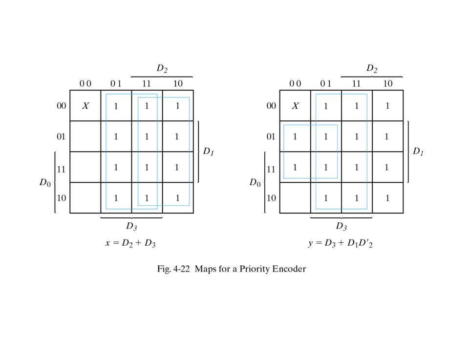
2-bit Priority Encoder A priority encoder is an encoder circuit that includes priority function. It means if two or more inputs are equal to 1 at the same time, the input having higher subscript number, considered as a higher priority. For example if D3 is 1 regardless of the value of the other input lines the result of output is 3 which is 11. If all inputs are 0, there is no valid input. For detecting this situation we considered a third output named V. V is equal to 0 when all input are 0 and is one for rest of the situations of TT.

31
2-bit Priority Encoder By using TT and K-map we get following boolean functions for 4-input (or 2-bit) priority encoder: X = D2 + D3 Y = D3 + D1D’2 V= D0 + D1 + D2 + D3 See next two slides for K-maps and the logic circuit of 2-bit priority encoder

34
Multiplexer It is a combinational circuit that selects binary information from one of the input lines and directs it to a single output line Usually there are 2n input lines and n selection lines whose bit combinations determine which input line is selected For example for 2-to-1 multiplexer if selection S is zero then I0 has the path to output and if S is one I1 has the path to output (see the next slide)
")
35
2-to-1 multiplexer

37
Boolean function Implementation
Another method for implementing boolean function is using multiplexer For doing that assume boolean function has n variables. We have to use multiplexer with n-1 selection lines and 1- first n-1 variables of function is used for data input 2- the remaining single variable ( named z )is used for data input. Each data input can be z, z’, 1 or 0. From truth table we have to find the relation of F and z to be able to design input lines. For example : f(x,y,z) = ∑(1,2,6,7)
is used for data input. Each data input can be z, z’, 1 or 0. From truth table we have to find the relation of F and z to be able to design input lines. For example : f(x,y,z) = ∑(1,2,6,7)")
39
F A,B,C,D = ∑(1,3,4,11,12,13,14,15)
")
40
Three-State Gates Three state gates exhibit three states instead of two states. The three states are: high : 1 Low : 0 High impedance : In that state the output is disconnected which is equal to open circuit. In the other words in that state circuit has no logic significant. We can have AND or NAND tree-state gates but the most common is three-state buffer gate

41
Three-State Gates We may use conventional gates such as AND or NAND as tree-state gates but the most common is three-state buffer gate. Note that buffer produces transfer function and can be used for power amplification. Three state buffer has extra input control line entering the bottom of the gate symbol (see next slide)
")
42
Three-state buffer C A Y z z

43
Three-state buffers can be used to implement
multiplexer

Similar presentations


>")


