Download presentation
Presentation is loading. Please wait.

1
Some Thoughts on L1 Pixel Trigger Wu, Jinyuan Fermilab April 2006

2
Introduction Preference on detector layout and related pattern recognition issues. Experience from Fermilab BTeV. –T–Triplet. –T–Triplet finding. –T–Tiny Triplet Finder. Data output rate of the readout chip. Triggering on “low PT” features.

3
Preference on Detector Layout

4
If N layers of pixel detector planes are affordable, (in terms of material, cost, data volume, power, cooling etc.), normally spaced configurations like (b) is more preferable. Pattern recognition for (b) is more difficult. From BTeV works, the pattern recognition for (b) is not as hard as we thought several years ago. (a) (b)
 is more difficult. From BTeV works, the pattern recognition for (b) is not as hard as we thought several years ago. (a) (b).")
5
BTeV and CMS-SLHC Pattern Recognition

6
Simulated B event in BTeV Silicon Pixel Detector

7
BTeV Level 1 Vertex Trigger -- Finding Triplets and Then … FPGA segment finders Merge Trigger decision to Global Level 1 Switch: sort by crossing number track/vertex farm (~2500 processors) 30 station pixel detector
 30 station pixel detector")
8
Triplets Triplet: –D–Data item with 2 free parameters. –#–# of measurements - # of constraints = 2. –A–A triplet is not necessarily a straight track segment. –A–A triplet may have more than 3 measurements. Circular track with known interaction point is a triplet since it has 2 free parameters. (Otherwise it has 3 parameters.)
.")
9
Three layers of nested loops are needed if the process is implemented in software. A total of n 3 combinations must be checked (e.g. 5x5x5=125). In FPGA, to “unroll” 2 layers of loops, large silicon resource may be needed without careful planning: O(N 2 ) Triplet Finding Plane APlane BPlane C for (i=0; i<N_A; i++){ for (j=0; j<N_B; j++){ for (k=0; k<N_C; k++){ }
. In FPGA, to unroll 2 layers of loops, large silicon resource may be needed without careful planning: O(N 2 ) Triplet Finding Plane APlane BPlane C for (i=0; i<N_A; i++){ for (j=0; j<N_B; j++){ for (k=0; k<N_C; k++){ }.")
10
Triplet Finding Triplet finding can be done in software or in firmware. Tiny Triplet Finder (TTF) is a firmware implementation developed in Fermilab BTeV. Tiny = small silicon usage. For more info on TTF, see handout. O(n 3 ) Software Processes O(n) FPGA Firmware Functions O(N 2 ) Implementations Hough Trans., etc. O(N*log(N)) Implementation Tiny Triplet Finder
 is a firmware implementation developed in Fermilab BTeV. Tiny = small silicon usage. For more info on TTF, see handout. O(n 3 ) Software Processes O(n) FPGA Firmware Functions O(N 2 ) Implementations Hough Trans., etc. O(N*log(N)) Implementation Tiny Triplet Finder.")
11
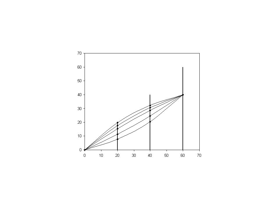
Circular Tracks from Collision Point on Cylindrical Detectors For a given hit on layer 3, the coincident between a layer 2 and a layer 1 hit satisfying coincident map signifies a valid circular track. A track segment has 2 free parameters, i.e., a triplet. The coincident map is invariant of rotation. 1 - 3 )+64 2 - 3 )+64
+64 2 - 3 )+64.")
12
Tiny Triplet Finder Reuse Coincident Logic via Shifting Hit Patterns C1 C2 C3 One set of coincident logic is implemented. For an arbitrary hit on C3, rotate, i.e., shift the hit patterns for C1 and C2 to search for coincidence.

13
Tiny Triplet Finder for Circular Tracks *R1/R3 *R2/R3 Triplet Map Output To Decoder Bit Array Shifter Bit Array Shifter Bit-wise Coincident Logic 1.Fill the C1 and C2 bit arrays. (n1 clock cycles) 2.Loop over C3 hits, shift bit arrays and check for coincidence. (n3 clock cycles)
 2.Loop over C3 hits, shift bit arrays and check for coincidence. (n3 clock cycles).")
14
Readout Chip Issues

15
Data Rate of Readout Chips SLHC: –80MHz –4 hits/(1.28cm) 2 (hits or clusters? cluster = 2.5 hits from BTeV. So 4 hits = 1.5 clusters) –16-bit/hit –3.125 Gb/cm 2 /s, with 8b10b etc. 5 Gb/cm 2 /s FPIX2 readout chip at Fermilab BTeV: –Area: 128x0.05mm x 22x0.4mm = 0.56cm 2. –Output: 6x140Mb/s = 840Mb/s. –1.5 Gb/cm 2 /s. If we redesign FPIX: –8x320Mb/s=2.56Gb/s; –4.57 Gb/cm 2 /s
 –16-bit/hit –3.125 Gb/cm 2 /s, with 8b10b etc. 5 Gb/cm 2 /s FPIX2 readout chip at Fermilab BTeV: –Area: 128x0.05mm x 22x0.4mm = 0.56cm 2. –Output: 6x140Mb/s = 840Mb/s. –1.5 Gb/cm 2 /s. If we redesign FPIX: –8x320Mb/s=2.56Gb/s; –4.57 Gb/cm 2 /s.")
16
Core Periphery FPIX2 Readout Chip Pixel Size: 50 m x 400 m Columns: 22 Rows: 128 Outputs: 1,2,4 or 6 Cu pairs @140MHz

17
Core Organization Column-based architecture Three mutually-dependent parts: –C–Core Logic –E–End-of-column Logic –P–Pixel Cells Readout order: –H–Hit cell by hit cell in a column. –C–Column by column. –N–Not time ordered.

18
Pixel Cell

19
Output of FPIX2 for BTeV b04b03b02b01b00b09b08b07b06b05b14b13b12b11b10b15b20b19b18b17b16b23b22b21 RowColumnBCO(7:0)ADC1 Hit24 1Status000 Sync24 00XXX Invalid coding: 111X0 A hit is output using 24 bits, @140Mb/s per Cu pair. User protocol is used as shown (not 8B/10B). The BCO field takes 8 bits. (+16 bits = 24 bits) To eliminate or reduce number of bits taken by the BCO, the chip has to be redesigned to output time ordered data. Doable or not? It is possible but not obvious now. FPIX1 was designed with time ordered data, but was slow. Study is needed.
. The BCO field takes 8 bits. (+16 bits = 24 bits) To eliminate or reduce number of bits taken by the BCO, the chip has to be redesigned to output time ordered data. Doable or not. It is possible but not obvious now. FPIX1 was designed with time ordered data, but was slow. Study is needed..")
20
Trigger/DAQ System Model

21
A Model of Trigger/DAQ System The readout chips send hit data to the correlation logic module (CLM, ~Correlator/OptoTX [J. Jones]) just outside detector via copper links. The CLM find triplets and send initial angle, momentum of each triplet to L1. L1 system issues trigger commands back. Readout chip send full data of selected BX to HLT/DAQ via CLM. Readout Chip Correlation Logic Module L1 10 m, Cu100 m, fiber Readout Chip Readout Chip Readout Chip HLT/ DAQ Triplet Data L1 Trigger Commands Full Data Outsider of Steel?
 just outside detector via copper links. The CLM find triplets and send initial angle, momentum of each triplet to L1. L1 system issues trigger commands back. Readout chip send full data of selected BX to HLT/DAQ via CLM. Readout Chip Correlation Logic Module L1 10 m, Cu100 m, fiber Readout Chip Readout Chip Readout Chip HLT/ DAQ Triplet Data L1 Trigger Commands Full Data Outsider of Steel .")
22
Output of the Readout Chip Data volume from the readout chips is large. (Full rate 3.125 Gb/cm 2 /s) Optionally, partial data can be sent to reduce the bandwidth (about (1/5)* 3.125 Gb/cm 2 /s) since the CLM needs only: – coordinate with lower resolution (1/2) –of a hit cluster (1/2.5). Study on readout chip re-design is needed. Readout Chip Correlation Logic Module 10 m, Cu Readout Chip Readout Chip Readout Chip RowColumnBCO(7:0)ADC1 Hit24 b04b03b02b01b00b09b08b07b06b05b14b13b12b11b10b15b20b19b18b17b16b23b22b21
 Optionally, partial data can be sent to reduce the bandwidth (about (1/5)* Gb/cm 2 /s) since the CLM needs only: – coordinate with lower resolution (1/2) –of a hit cluster (1/2.5). Study on readout chip re-design is needed. Readout Chip Correlation Logic Module 10 m, Cu Readout Chip Readout Chip Readout Chip RowColumnBCO(7:0)ADC1 Hit24 b04b03b02b01b00b09b08b07b06b05b14b13b12b11b10b15b20b19b18b17b16b23b22b21.")
23
L1 Trigger Commands The CLM find triplets and send initial angle, momentum of each triplet to L1 and L1 system issues a multi-bit trigger commands back. Readout chip send full data of selected BX to HLT/DAQ via CLM. The data volume of the selected BX is relatively small. Optionally, the correlation logic module can run one or a few longer algorithms (L1.5?) when the full data flow through. The HLT uses the results when making L2 decisions. So the multi-bit trigger command = {BX, L1.5 algorithm ID}: Dump data in 1234 and apply algorithm ABCD. 10 m, Cu100 m, fiberOutsider of Steel? Readout Chip Correlation Logic Module L1 Readout Chip Readout Chip Readout Chip HLT/ DAQ Triplet Data L1 Trigger Commands Full Data
 when the full data flow through. The HLT uses the results when making L2 decisions. So the multi-bit trigger command = {BX, L1.5 algorithm ID}: Dump data in 1234 and apply algorithm ABCD. 10 m, Cu100 m, fiberOutsider of Steel. Readout Chip Correlation Logic Module L1 Readout Chip Readout Chip Readout Chip HLT/ DAQ Triplet Data L1 Trigger Commands Full Data.")
24
More Readout Chip Issues, Latency etc.

25
Tiny Triplet Finder for Circular Tracks *R1/R3 *R2/R3 Triplet Map Output To Decoder Bit Array Shifter Bit Array Shifter Bit-wise Coincident Logic 1.Fill the C1 and C2 bit arrays. (n1 clock cycles) 2.Loop over C3 hits, shift bit arrays and check for coincidence. (n3 clock cycles)
 2.Loop over C3 hits, shift bit arrays and check for coincidence. (n3 clock cycles).")
26
Latency Budget Usage for Triplet Finding Process CMS L1 decision time = 6.4 s, 2 x 0.5 s of it will be in cable delay. Filling the C1 and C2 bit arrays takes n1 clock cycles. Looping over C3 hits, shifting bit arrays and checking for coincidence take n3 clock cycles + # pipeline stages (about 10). Assume n1, n3 = 64, latency usage = 64 + 64 + 10 = 138 clock cycles. At 160 MHz (FPGA or ASIC) clock frequency, 138 clock cycles = 138/(160*6.4) = 13% (of 6.4 s CMS L1 decision time). This is only an example, but looks OK.
. Assume n1, n3 = 64, latency usage = = 138 clock cycles. At 160 MHz (FPGA or ASIC) clock frequency, 138 clock cycles = 138/(160*6.4) = 13% (of 6.4 s CMS L1 decision time). This is only an example, but looks OK..")
27
A Closer View of Latency Budget The readout chips send out hit data to the Correlation Logic Module. The triplet finding starts after receiving data of the first hit. After all hits are transmitted, phase 2 of triplet finding (looping over C3 hits, shifting bit arrays and checking for coincidence) runs. Triplet data are sent out after first triplet is found. After cable delay, the L1 starts L1 processes after receiving first triplet data. After all triplet data are received, the L1 command is issued. The L1 command is sent back and executed. Readout Chip Correlation Logic Module L1 Readout Chip Triplet Data L1 Trigger Commands Output Hits Triplet Finding (1)Triplet Finding (2) Triplet Data Out Cable (1)Cable (2)L1 Processes Cable (1) L1
 runs. Triplet data are sent out after first triplet is found. After cable delay, the L1 starts L1 processes after receiving first triplet data. After all triplet data are received, the L1 command is issued. The L1 command is sent back and executed. Readout Chip Correlation Logic Module L1 Readout Chip Triplet Data L1 Trigger Commands Output Hits Triplet Finding (1)Triplet Finding (2) Triplet Data Out Cable (1)Cable (2)L1 Processes Cable (1) L1.")
28
Max # of Hits/BX 4 hits/(1.28cm) 2 /BX is an average, in some BX, the # of hits may be many times larger. The readout chip should drop some hits if the # of hits/BX is too big or the time to output hits will be too long. (Note the 6.4 s L1 latency.) Consider 64, 128, 256 hits/(1.28cm) 2 /BX, i.e., x16, x32, x64 of average, the time to output the hits takes 16, 32, 64 BX on link with throughput match the average data rate. The output time: 0.2 s, 0.4 s, 0.8 s -- should be OK. Output Hits Triplet Finding (1)Triplet Finding (2) Triplet Data Out Cable (1)Cable (2)L1 Processes Cable (1) L1
 Consider 64, 128, 256 hits/(1.28cm) 2 /BX, i.e., x16, x32, x64 of average, the time to output the hits takes 16, 32, 64 BX on link with throughput match the average data rate. The output time: 0.2 s, 0.4 s, 0.8 s -- should be OK. Output Hits Triplet Finding (1)Triplet Finding (2) Triplet Data Out Cable (1)Cable (2)L1 Processes Cable (1) L1.")
29
Readout Chip Spec Should read out time ordered data. Should drop data gracefully if # of hits/BX is too big. Should drop data gracefully if # of hits/ several BX (a short term average) is too big. Should be able to output both brief data for trigger and full data for readout. Should store data on chip for 6.4 s. ?
 is too big. Should be able to output both brief data for trigger and full data for readout. Should store data on chip for 6.4 s. .")
30
Extra Possibility: Triggering on Low PT Features

31
Triggering on “Low PT” Features? Many tracking algorithms degrade rapidly when momentum of the track goes low. Circular track triplet finding does not need high PT assumption, so it does not degrade as rapidly. The trigger system discussed is especially suitable if one needs to trigger on low PT features of the event. In CMS 4T B field, all tracks look to be “low PT”.

32
Example: Finding “Soft Jets” A simulated event with 200 tracks. Flat distributions. Min. R = 55 cm 8+8 soft tracks are added. They are grouped in 2 small initial angle regions, i.e., 2 “soft jets”. Can you see the “soft jets”? Can you see the “soft jets” now? Track Initial Angle Distributions

33
Summary

34
With experience from Fermilab BTeV on triplet finding, pattern recognition is not a problem. One should feel free to choose preferred detector layout. Data output rates of the current readout chips are close enough to the SLHC requirement. But studies are needed. Triggering on “low PT” features is possible. But studies are needed.

35
The End Thanks

Similar presentations
 for U.H., M. Narain (Brown U) M. Johnson, R. Lipton (Fermilab) E. Hazen, S.X. Wu, (Boston.>")


 at DØ Beauty 2005 in Assisi, June 2005 Sascha Caron for the DØ collaboration Tag beauty fast …>")

>")

>")


 combinations must be checked. Hash Sorter - Firmware Implementation and an Application for the Fermilab BTeV Level 1.>")


