Download presentation
Presentation is loading. Please wait.

1
Input electron-optics of a photomultiplier with (a) focusing dynodes and (b) venetian-blind dynodes, showing equipotential lines and electron trajectories (a) (b) The input system must satisfy two main requirements: − It must be able to focus the maximum number of electrons onto the first dynode regardless of their initial velocity and regardless of where on the photocathode they originate. The ratio between the number of electrons reaching the useful area of the first dynode and the total number of electrons emitted by the cathode is called the collection efficiency; it varies with wavelength but is usually greater than 80%. − The transit time of electrons between the cathode and the first dynode must, as far as possible, be independent of their initial velocity and point of origin. This is particularly important in fast-response photomultipliers, and these therefore have more complex input systems. Electron-optical input system

2
When designing a photomultiplier tube, the electron trajectory from the photocathode to the first dynode must be carefully designed in consideration of the photocathode shape (planar or spherical window), the shape and arrangement of the focusing electrode and the supply voltage, so that the photoelectrons emitted from the photocathode are efficiently focused onto the first dynode. The collection efficiency of the first dynode is the ratio of the number of electrons landing on the effective area of the first dynode to the number of emitted photoelectrons. In some applications where the electron transit time needs to be minimized, the electrode should be designed not only for optimum configuration but also for higher electric fields than usual. Function of λ and voltage 1° dynode

3
Types of Photocatode

4
Circular-cage, box-and-grid, and linear-focused dynode structures Circular-cage type side-on type Box-and-grid type head-on type Linear- focused type transmission mode Compactness Time response Collection efficiency uniforminty Time resolution linearity

5
Mesh-type Microchannel Plate Time, position Metal Channel type Simple design, collection for large area Parallel electric Field Magnetic field parallel Anode Position proximity Short electron path, proximity, magnetic And time resolution Time, power photon counting

8
Fast-response tubes For fast response photomultipliers, there is an additional requirement, namely to keep transit time variations in the cathode/first-dynode space to a minimum. Two components: -a chromatic component, due to the spread of initial velocities of electrons originating from the same point. The initial velocity vector can be resolved into a velocity v n normal to the cathode, corresponding to an energy E n, and a velocity v t tangential to the cathode, corresponding to an energy E t. -a geometric component, due to the difference in transit times between primary paths of different lengths from different points on the cathode; a contributing factor is the inhomogeneity of the electric field in the space traversed by the electrons. Minimizing differences between the electron path lengths in the cathode/first-dynode space. In fast-response photomultipliers this is done by using a concave cathode and one or more additional focusing electrodes.

9
Fast-response tubes − a chromatic component, due to the spread of initial velocities. The initial velocity vector can be resolved into a velocity v n normal to the cathode, and a velocity v t tangential to the cathode. - a geometric component, due to the difference in transit times between primary paths of different lengths from different points on the cathode; a contributing factor is the inhomogeneity of the electric field in the space traversed by the electrons.

10
Relative distribution of photoelectron energies, E ph, from a layer of SbKCs at 290 °K, for incident photon energies (a) from 2.15 eV to 3.06 eV, and (b) from 4.28 eV to 5.12 eV Photoelectron energy distribution (in electrons per photon per eV) from a layer of GaAs(Cs) for incident-photon energies (a) from 1.4 eV to 2.2 eV, and (b) from 1.8 eV to 3.2 eV NEA Important NEA effect
 from 2.15 eV to 3.06 eV, and (b) from 4.28 eV to 5.12 eV Photoelectron energy distribution (in electrons per photon per eV) from a layer of GaAs(Cs) for incident-photon energies (a) from 1.4 eV to 2.2 eV, and (b) from 1.8 eV to 3.2 eV NEA Important NEA effect")
11
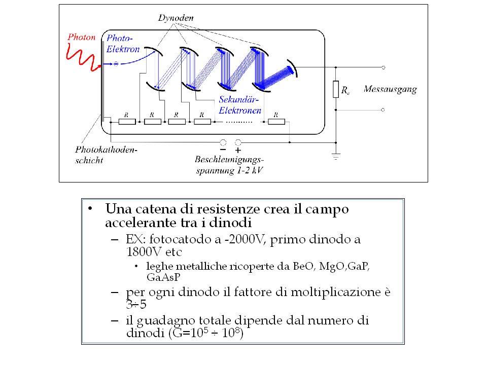
Electron Multiplier (Dynode Section) Photoelectrons emitted from the photocathode are multiplied by the first dynode through the last dynode (up to 19 dynodes), with current amplification ranging from 10 to as much as 10 8 times, and are finally sent to the anode. Major secondary emissive materials used for dynodes are alkali antimonide, beryllium oxide (BeO), magnesium oxide (MgO), gallium phosphide (GaP) and gallium phosphide (GaAsP). These materials are coated onto a substrate electrode made of nickel, stainless steel, or copper-beryllium alloy. When a primary electron with initial energy Ep strikes the surface of a dynode, δ secondary electrons are emitted. This δ, the number of secondary electrons per primary electron, is called the secondary emission ratio.
, magnesium oxide (MgO), gallium phosphide (GaP) and gallium phosphide (GaAsP). These materials are coated onto a substrate electrode made of nickel, stainless steel, or copper-beryllium alloy. When a primary electron with initial energy Ep strikes the surface of a dynode, δ secondary electrons are emitted. This δ, the number of secondary electrons per primary electron, is called the secondary emission ratio..")
13
Guadagno Il guadagno di un p.m. dipende dal numero di dinodi nel sistema di moltiplicazione e dal fattore di emissione secondaria , che è funzione dell’energia dell’elettrone primario. Infatti l’energia di un elettrone incidente è funzione della differenza di potenziale tra i dinodi V d. k costante di proporzionalità Assumendo che la differenza di potenziale applicata è ugualmente suddivisa tra i dinodi, il guadagno complessivo del p.m. è: Fissata una d.d.p minima V b, si può calcolare il numero degli stadi (dinodi) n necessari per ottenere un determinato guadagno G: Variazione del guadagno rispetto alla differenza di potenziale fornita: Se n=10, G varia del 10% per una variazione di V b dell’1% Tensione catodo-anodo
 n necessari per ottenere un determinato guadagno G: Variazione del guadagno rispetto alla differenza di potenziale fornita: Se n=10, G varia del 10% per una variazione di V b dell’1% Tensione catodo-anodo.")
14
Gain vs. supply voltage

15
Photocurrent variation as a function of cathode-to-first- dynode voltage, with relative incident flux as parameter As the first dynode is made more positive with respect to the photocathode, the photocurrent tends towards a saturation value. Depending on the type of photomultiplier, the saturation voltage is between a few volts and a few tens of volts. The saturation current is proportional to the incident flux.

16
Statistical broadening of secondary electron yeld from the first dynode as a function of incident photoelectron number Major secondary emissive materials used for dynodes are alkali antimonide, beryllium oxide (BeO), magnesium oxide (MgO), gallium phosphide (GaP) and gallium phosphide (GaAsP). These materials are coated onto a substrate electrode made of nickel, stainless steel, or copper- beryllium alloy. Difficult photon counting:

17
Peaks corrisponding to number of photoelectrons

20
Condizioni per la progettazione del divisore di tensione -sulla corrente media continua nel divisore (determinazione delle resistenze) -sulla corrente di picco negli ultimi stadi del divisore (determinazione delle capacita’)
 -sulla corrente di picco negli ultimi stadi del divisore (determinazione delle capacita’)")
21
To ensure that voltage variations due to anode current variations are negligible, the nominal divider current Ip must be much larger than Ia; a good rule is: Ip > 100 Ia Consider a type C voltage distribution with V HT = 2500 V, an interdynode voltage increment Vd, and a division ratio such that there are precisely 21 such increments. Suppose that the mean anode current Ia is 10 μA. The divider current Ip must then be at least 1 mA, which means a total divider resistance of 2.5 MΩ and an incremental resistor value of 2.5 × 10 6 /21 ≈ 120 kΩ (resistore incrementale) Zener diodes can substitute some of resistors in the divider to keep certain inter-electrode voltages constant. 1)-Between the dynodes of the first two multiplier stages to keep the gains of those stages constant. 2)-Another place to use zener diodes is in the last stages of the divider, to stabilize the voltages there throughout a wider range of anode current variations. Only zener, no regulation.
 Zener diodes can substitute some of resistors in the divider to keep certain inter-electrode voltages constant. 1)-Between the dynodes of the first two multiplier stages to keep the gains of those stages constant. 2)-Another place to use zener diodes is in the last stages of the divider, to stabilize the voltages there throughout a wider range of anode current variations. Only zener, no regulation..")
22
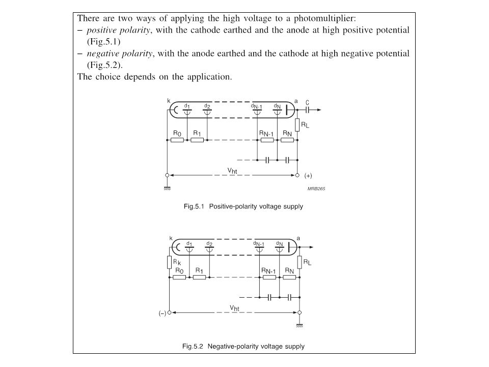
The interstage voltage for each electrode is supplied by using voltage-dividing resistors (100 kΩ to 1 MΩ) connected between the anode and cathode. Sometimes Zener diodes are used with voltage-dividing resistors as shown in Figure 2. Ip = V(HV) / (R1+R2+···+R6+R7) The divider current Ib is the applied voltage V divided by the sum of resistor values as follows Ip = V(HV)-(Sum of voltages generated at Dz1 to Dz4) / R1+R2+R3 The Zener diodes (Dz) shown in Figure 2 are used to maintain the interstage voltages at constant values for stabilizing the photomultiplier tube operation regardless of the magnitude of the cathode-to-anode supply voltage. In this case, Ib is obtained by using The capacitors C1, C2, C3 and C4 connected in parallel with the Zener diodes serve to minimize noise generated by the Zener diodes. This noise becomes significant when the current flowing through the Zener diodes is insufficient.
 / (R1+R2+···+R6+R7) The divider current Ib is the applied voltage V divided by the sum of resistor values as follows Ip = V(HV)-(Sum of voltages generated at Dz1 to Dz4) / R1+R2+R3 The Zener diodes (Dz) shown in Figure 2 are used to maintain the interstage voltages at constant values for stabilizing the photomultiplier tube operation regardless of the magnitude of the cathode-to-anode supply voltage. In this case, Ib is obtained by using The capacitors C1, C2, C3 and C4 connected in parallel with the Zener diodes serve to minimize noise generated by the Zener diodes. This noise becomes significant when the current flowing through the Zener diodes is insufficient..")
23
Linearity Current is the difference between the divider current Ib and the dynode current IDy flowing in the opposite direction through the voltage- divider resistor. The anode current and dynode current flow act to reduce the divider current and the accompanying loss of the interstage voltage. The reduction of the divider current can be ignored if the anode output current is small. Influence of photocurrent on voltage applied to each electrode The maximum practical anode current in a DC output is usually 1/20th to 1/50th of the divider current. If linearity better than ±1 percent is required, the maximum output must be held to less than 1/100th of the divider current.

24
Anode linearity The anode linearity is limited by two factors: the voltage-divider circuit and space charge effects due to a large current flowing in the dynodes. Linearity Pulse mode : Limited by the space charge effects. DC mode : Limited by a change in the voltage divider due to the magnitude of signal current. When an intense light pulse enters a photomultiplier tube a large current flows in the latter dynode stages, increasing the space charge density, and causing current saturation. Any dynode type provides better pulse linearity, when the electric field strength between each dynode is enhanced. Relationship between the pulse linearity and the supply voltage A good rule is to ensure that the ratio Ia/Ip ≤ 0.01

25
When a photomultiplier tube is pulse-operated using the voltage-divider circuit the maximum linear output is limited to a fraction of the divider. To prevent this problem, decoupling capacitors can be connected to the last few stages, as shown: If the output-pulse peak voltage is V0, and the pulse width is T W and the load resistance is RL, the output pulse charge Q0 per pulse is expressed by: If we let the charge stored in capacitor C3 be Q3, then to achieve good output linearity of better than percent, the following relation should generally be established: from the common relation of Q 0 =CV 3, affinche la linearita’ cambi del % e quindi V 3 cambi del % Q 0 =C 3 xV 3 /100

26
The charges Q2 and Q1 stored in C2 and C1 respectively are calculated by assuming that δ between each dynode is 2-3, as follows: Then, the capacitance values of C2 and C1 can be obtained in the same way as in C3.

27
Here, as an example, with the output pulse peak voltage V0=50 mV, pulse width T W =1 μs, load resistance RL=50 Ω, interstage voltages V3=V2=V1=100 V, each capacitor value can be calculated in the following steps: The capacitance values required of the decoupling capacitors C3, C2 and C1 are calculated respectively as follows: The above capacitance values are minimum values required for proper operation. It is therefore suggested that the voltage divider circuit be designed with a safety margin in the capacitance value, of about 10 times larger than the calculated values. If the output current increases further, additional decoupling capacitors should be connected as necessary to the earlier stages, as well as increasing the capacitance values of C1 to C3.

28
Corrente nel divisore di corrente = 1,6 mA Utimi 3 stadi alla stessa tensione

29
Even under conditions where adequate countermeasures for pulse output linearity have been taken by use of decoupling capacitors, output saturation will occur at a certain level as the incident light is increased. This is caused by an increase in the electron density between the electrodes, causing space charge effects which disturb the electron current. As a corrective action to overcome space charge effects, the voltage applied to the last few stages, where the electron density becomes high, should be set at a higher value than the standard voltage distribution so that the voltage gradient between those electrodes is enhanced. For this purpose, a so-called tapered voltage-divider circuit is often employed, in which the interstage voltage is increased in the latter stages. Pulse output linearity countermeasures using decoupling capacitors and tapered voltage-divider circuit

30
The voltage distribution ratio for the latter stages near the anode is an important factor that determines the output linearity of a photomultiplier tube. In contrast, the voltage distribution between the cathode, focusing electrode and first dynode has an influence on the photoelectron collection efficiency and the secondary emission ratio of the first dynode. These parameters are major factors in determining the output signal-to-noise ratio, pulse height dispersion in the single and multiple photon regions, and also electron transit time spread Voltage-divider circuit with tapered configurations at both the earlier and latter stages

31
Linearity characteristic using a tapered and a normal voltage-divider circuit The linearity can be improved by use "a tapered voltage-divider") designed to increase the interstage voltages at the latter dynode stages. Figure shows a comparison of pulse linearity characteristics measured with a tapered voltage-divider circuit versus that of a normal voltage divider circuit. It is obvious that pulse linearity is improved about 10 times by using the tapered voltage-divider circuit. Note that when this type of tapered voltage-divider circuit is used, the anode output lowers to about 1/3rd to 1/5th in comparison with the normal voltage-divider anode output.

32
Voltage-divider circuit using transistors The photoelectron current first flows into the first dynode, then secondary electrons flow through the successive dynodes and into the collector of each transistor. As a result, the emitter potential of each transistor increases while the collector current decreases along with a decrease in the base current. At this point, the decrease in the collector current is nearly equal to the current flowing through the photomultiplier tube and accordingly, the transistors supply the current for the photomultiplier tube. BJT divider

33
Fotomoltiplicatore = Generatore di corrente

Similar presentations


 Energy (J) Irradiance (W/m 2 ) Emittance (W/m 2 ) Intensity (W/sr) Radiance (W/sr m 2 )>")


 What characteristics should we look for in a transducer?>")


: the number of components in an integrated circuit will double every year;>")
 Dr. Zainal Salam, UTM-JB 1 Chapter 3 DC to DC CONVERTER (CHOPPER) General Buck converter Boost converter.>")

