Download presentation
Presentation is loading. Please wait.

2
Propagation Delay: capacitances introduce delay
All physical devices have delays due to the charging and discharging of (parasitic capacitors) and interconnection resistance. flow Resistive tube Crossing lines level t Propagation delay tpd
 and interconnection resistance. flow. Resistive tube. Crossing lines. level. t. Propagation delay. tpd.")
3
Where to these capacitors come from?
Most are parasitic caps 2um passivation M9 M8 M7 M6 M5 M4 M3 M2 M1 (Source: TSMC) Cross section of Altera Stratix EP1S25 (TSMC process) Crossing lines Crossing interconnections (Source: IBM) 9 level of interconnections
 Cross section of Altera Stratix EP1S25 (TSMC process) Crossing lines. Crossing interconnections. (Source: IBM) 9 level of interconnections.")
4
Review: 6-3 Flip-Flop Timing Parameters and metastability
Edge triggered flip-flop If one violates the set-up time and hold time, the flip-flop can go in a metastable state. C D Q In Out C tS th In (D) set-up time hold time
 set-up time. hold time.")
5
Metastable behavior Example of metastable behavior:
After a while the flip-flop will go into a stable state (randomly). If this happens before the next clock edge, the actual circuits will see a defined input. The longer the clock period is the less chance of synchronization failure. Or use two synchronization flip-flops in series metastable Eventually, the flip-flop will settle (Oscilloscope trace)
. If this happens before the next clock edge, the actual circuits will see a defined input. The longer the clock period is the less chance of synchronization failure. Or use two synchronization flip-flops in series. metastable. Eventually, the flip-flop will settle. (Oscilloscope trace)")
6
Practical Considerations
Debouncing Practical Considerations

7
Practical considerations
In many cases the input signals come from push buttons and sensors: Switches exhibit bouncing Are not synchronous Give multiple input (sampled many times) This can give catastrophic failures of timing problems Solutions: Debounce the switch Synchronizer One-pulse circuit (and synchronizer)
 This can give catastrophic failures of timing problems. Solutions: Debounce the switch. Synchronizer. One-pulse circuit (and synchronizer)")
8
Bouncing of switches What is bouncing?
When closing a switch, the switch contact bounces back and forth, giving multiple pulses Measured signal A B chip Push button switch 5V Causes spurious glitches on input B

9
Debouncing circuit The two resistors will keep S=R=0:
Inputs are never floating Output does not bounce Push switch R 5V 1 2 Q R S S Q contact to 5V Bouncing No bouncing SR latch Is set S=R=0 No change

10
Issues with asynchronous inputs
Likely violation of set up times Issues with asynchronous inputs

11
Asynchronous inputs Asynchronous inputs (e.g. from sensors) can cause timing problems if set up time is violated: Use a synchronizer Signal from sensor CLK tS setup time This setup time violation can give problems, such as metastability and erroneous operation: stable metastable

12
Metastability and Synchronization
A flip-flop can get into a metastable state: When the set-up or hold times are violated This can happen for asynchronous inputs (e.g. push button; sensor input, etc) Input CLK Q0 Q1 D Q D0i Q0 Sensor asynchronous input D1 Q1 CLK Both flip flops behave differently! kick Q0 kick Q1
 Input. CLK. Q0. Q1. D. Q. D0i. Q0. Sensor asynchronous input. D1. Q1. CLK. Both flip flops behave differently! kick. Q0. kick. Q1.")
13
Metastability (continued)
Asynchronous inputs: Use a synchronizing flip-flop Now, only the synchronizer may get into the metastable state; however, there is a good chance that by the end of the clock period it went into one of the stable states. D Q D0 Q0 D1i Q1 Di Ai Synchronizer Asynchronous input

14
Synchronizer Di Ai Sensor,async Synchronized output CLK CLK
Q Di Ai CLK Sensor,async Synchronized output Signal from sensor CLK Synchronized output Note: by having the sensor input enter through a single D flip-flop the problem of timing circuits is reduced greatly (there is still a small chance that the D FF will be unstable). By using two D flip-flops in series one further reduces the risk that the 2nd FF will be metastable.
. By using two D flip-flops in series one further reduces the risk that the 2nd FF will be metastable.")
15
Registers and Register Transfers
Chapter 7 Registers and Register Transfers (Source: reference.findtarget.com)
")
16
7-1 Registers Register – a collection of flip-flops, together with some combinational logic, that performs data processing tasks (e.g. storing, moving data, etc). In theory, a register is sequential logic which can be defined by a state table. More often think of a register as storing a vector of binary values.
. In theory, a register is sequential logic which can be defined by a state table. More often think of a register as storing a vector of binary values.")
17
Simple Storage Register
A D flip-flop register loads information on every clock cycle! To “store” or “load” information should be controlled by a signal. inputs Outputs Active low Clear (asynch)
")
18
Register with Parallel Load: Clock Gating
Use a signal to block the clock to the register Load is a frequent name for the signal that controls register storage and loading Load = 1: Load the values on the data inputs Load = 0: Store the values in the register Gated clock: To C input of Flip-flops Clock gating: 1 Clock Load Gated Clock to FF Timing: Extra edge!

19
Registers with Load-Controlled Feedback
A more reliable way to selectively load a register: Run the clock continuously, and Selectively use a load control to change the register contents. Example: 2-bit register with Load Control: For Load = 0, loads register contents (hold current values) For Load = 1, loads input values (load new values) Hardware more complex than clock gating, but free of timing problems 2-to-1 Multiplexers C D Q Clock In0 In1 A1 A0 Y1 Y0 Load
 For Load = 1, loads input values (load new values) Hardware more complex than clock gating, but free of timing problems. 2-to-1 Multiplexers. C. D. Q. Clock. In0. In1. A1. A0. Y1. Y0. Load.")
20
Registers with Load Control: Example
K1=1: R1 stores the result of addition/subtraction

21
7-2 Register Transfers The data is stored in registers, which compose the datapath. In many cases one wants to perform a variety of arithmetic and logical operations on a set of data bits (e.g. a 16-bit word): Additions, subtraction, shifting, loading, etc. (Source: reference.findtarget.com)
: Additions, subtraction, shifting, loading, etc. (Source: reference.findtarget.com)")
22
Register Transfers Operations
The type of operations on the data will be determined by a controller, often called a control unit. This division between the datapath and control unit makes the design of complex systems easier. Strategy: divide and conquer! Registers play a key role in complex digital systems! Transfers between registers determine the operations. (Source: reference.findtarget.com)
")
23
Datapath and Control Unit
Control signals Status signals Control Unit Datapath Determines which operation and sequence of operation based on status signals Control signals: activate various operations in the datapath Is a large finite state machine Stores data in registers Performs operations on data, specified by Cntr unit Provide status signals Is defined by registers and its operations: Register Transfer Operations (RTL) An elementary operation: microoperation
 An elementary operation: microoperation.")
24
7-3 Register Transfer Operations
Register Transfer Operations – The movement and processing of data stored in registers Three basic components: set of registers operations control of operations Elementary Operations -- load, count, shift, add, bitwise "OR", etc. Elementary operations called microoperations Register Notation: PC(H) PC(L) R2 Ex. 8-bit register R: 16-bit registers: R …1 0 LSB MSB
 PC(L) R2. Ex. 8-bit register R: 16-bit registers: R. 7 …1 0. LSB. MSB.")
25
Conditional Transfer R1 R2 K 1 Clock n Clock K1 Clock K1
If (K1 =1) then (R2 R1) is shortened to K1: (R2 R1) where K1 is a control variable specifying a conditional execution of the microoperation. R1 R2 K 1 Clock Load n Clock K1 Transfer occurs here No Transfers Occur Here Clock K1 Transfer occurs here No Transfers Occur Here
 then (R2 R1) is shortened to. K1: (R2 R1) where K1 is a control variable specifying a conditional execution of the microoperation. R1. R2. K. 1. Clock. Load. n. Clock. K1. Transfer occurs. here. No Transfers Occur Here. Clock. K1. Transfer occurs. here. No Transfers Occur Here.")
26
7-5 Microoperations Logical Groupings:
Transfer - move data from one set of registers to another Arithmetic - perform arithmetic on data in registers Logic - manipulate data or use bitwise logical operations Shift - shift data in registers Arithmetic operations + Addition – Subtraction * Multiplication / Division Logical operations (bitwise) Logical OR Logical AND Logical Exclusive OR Not
 Logical OR Logical AND Logical Exclusive OR Not.")
27
Example Microoperations
Add the content of R1 to the content of R2 and place the result in R1. R1 R1 + R2 Multiply the content of R1 by the content of R6 and place the result in PC. PC R1 * R6 Exclusive OR the content of R1 with the content of R2 and place the result in R1. R1 R1 R2

28
Example Microoperations (Continued)
On condition K1 OR K2, the content of R1 is Logic bitwise ORed with the content of R3 and the result placed in R1: (K1 + K2): R1 R1 R3 NOTE: "+" (as in K1 + K2) and means “OR.” In R1 R1 + R3, + means “plus.”
: R1 R1 R3. NOTE: + (as in K1 + K2) and means OR. In R1 R1 + R3, + means plus.")
29
Arithmetic Microoperations
Note that any register may be specified for source 1, source 2, or destination. These simple microoperations operate on the whole word Symbolic Designation Description R0 R1 + R2 Addition R1 Ones Complement R1 + 1 Two's Complement R2 + R2 minus R1 (2's Comp) Increment (count up) – 1 Decrement (count down)
 Increment (count up) – 1. Decrement (count down)")
30
Implementation of an Arithmetic Micro operation
Conditional microoperation: X K1 : R1 R1 + R2 X K1 : R1 R1 + R2 + 1 Condition

31
Logical Microoperations
Symbolic Description Designation R0 R1 Bitwise NOT R0 R1 Ú R2 Bitwise OR (sets bits) R0 R1 Ù R2 Bitwise AND (clears bits) R0 R1 Å R2 Bitwise EXOR (complements bits)
 R0. R1. Ù. R2. Bitwise AND (clears bits) R0. R1. Å. R2. Bitwise EXOR (complements bits)")
32
Logical Microoperations (continued)
Let R1 = , and R2 = Then after the operation, R0 becomes: (sets bits) (clears bits) (complements bits)
 (clears bits) (complements bits)")
33
Shift Microoperations
Let R2 = Then after the operation, R1 becomes: Symbolic Designation Description R1 sl R2 Shift Left sr R2 Shift Right R1 Operation sl R2 sr R2 Note: These shifts "zero fill". Sometimes a separate flip-flop is used to provide the data shifted in, or to “catch” the data shifted out. Other shifts are possible (rotates, arithmetic).
.")
34
7-6: Microoperation on a Single Register
MUX-based transfers Shift registers (needed for Lab) Ripple Counter Synchronous binary counter Other counters
 Ripple Counter. Synchronous binary counter. Other counters.")
35
7-6 Microoperations on a Single Register
The focus is on the implementation of microperations with a SINGLE register as the Destination of the results In addition to the register there is some combinational logic needed. This is considered part of the register and is called DEDICATED logic (in contrast to SHARED logic for multiple destination registers). Multiplexer-based transfer: makes use of multiplexers to allow multiple operations on a single destination register (See next)
. Multiplexer-based transfer: makes use of multiplexers to allow multiple operations on a single destination register (See next)")
36
Multiplexer-Based Transfers
Multiplexers connected to register inputs produce flexible transfer structures Consider the following circuit What are the corresponding Register Transfer operations of the following implementation? Load R0 n MUX S K 2 1 R2 R1 Combinational circuit

37
Register Transfer Operations implemented by the following circuit
K1.K2: R0 R1 K1.K2: R0 R2 Load R0 n MUX S K 2 1 R2 R1

38
Exercise Consider the following circuit (Note: Clocks are omitted for clarity) What are the corresponding Register Transfer operations? Load R0 n MUX S K 2 1 R2 R1 The transfers are: K1: R0 R K2.K1’: R0 R2

39
Shift Registers Shift Registers move data laterally within the register toward its MSB or LSB position In the simplest case, the shift register is simply a set of D flip-flops connected in a row like this: Data input, In, is called a serial input or the shift right input. Data output, Out, is often called the serial output. The vector (A, B, C, Out) is called the parallel output.
 is called the parallel output.")
40
Shift Registers (continued)
The behavior of the serial shift register is given in the listing on the lower right T0 is the register state just before the first clock pulse occurs T1 is after the first pulse and before the second. Initially unknown states are denoted by “?” Complete the last three rows of the table In A B C Out D Q D Q D Q D Q Clock CP Clock In A B C Out T0 ? T1 1 T2 T3 T4 T5 T6 ROW T4: 10110 Row T5: Row T6:

41
Shift Registers (continued)
A B C Out D Q D Q D Q D Q Clock CP CP In A B C Out T0 ? T1 1 T2 T3 T4 T5 T6 ROW T4: 10110 Row T5: Row T6: 1 1 1

42
Parallel Load Shift Registers
By adding a mux between each shift register stage, data can be shifted or loaded If SHIFT is low, A and B are replaced by the data on DA and DB lines, else data shifts right on each clock. By adding more bits, we can make n-bit parallel load shift registers. Register Transfer Operation: D Q A B CP SHIFT IN DA DB MUX SHIFT: Q sr Q SHIFT’: Q D

43
Parallel Load Shift Registers with Load
Q 2 1 S1 S0 Shift Load C Q0 Q1 Q2 D0 D1 D2 Serial input Control Use a multiplexer with 3 inputs: 2 1 S1 S0 Shift Load Serial input D0 =

44
Timing Register Transfer Operation: Shift: Q sl Q Shift.Load: Q D
Clock Load (Shift = 0) Di Qi Output changes here Register Transfer Operation: Shift: Q sl Q Shift.Load: Q D
 Di. Qi. Output changes here. Register Transfer Operation: Shift: Q sl Q. Shift.Load: Q D.")
45
Bidirectional shift register

46
Counters Counters are sequential circuits which "count" through a specific state sequence. They can count up, count down, or count through other fixed sequences. Two distinct types are in common usage: Ripple Counters Clock is connected to the flip-flop clock input on the LSB bit flip-flop For all other bits, a flip-flop output is connected to the clock input, thus circuit is not truly synchronous Output change is delayed more for each bit toward the MSB. Resurgent because of low power consumption Synchronous Counters Clock is directly connected to the flip-flop clock inputs Logic is used to implement the desired state sequencing

47
Ripple Counter How does it work? B
When there is a positive edge on the clock input of A, A complements The clock input for flip- flop B is the complemented output of flip-flop A When flip A changes from 1 to 0, there is a positive edge on the clock input of B causing B to complement Reset Clock D CR B A CP A B 1 2 3

48
Ripple Counter (continued)
The arrows show the cause-effect relation- ship from the prior slide => The corresponding sequence of states => (B,A) = (0,0), Each additional bit, C, D, …behaves like bit B, changing half as frequently as the bit before it. For 3 bits: (C,B,A) = (0,0,0), (0,0,1), (0,1,0), (0,1,1), (1,0,0), (1,0,1), (1,1,0), (1,1,1), (0,0,0), … CP B A 1 2 3 (0,1), (1,0), (1,1), (0,0), (0,1), …
 = (0,0), Each additional bit, C, D, …behaves like bit B, changing half as frequently as the bit before it. For 3 bits: (C,B,A) = (0,0,0), (0,0,1), (0,1,0), (0,1,1), (1,0,0), (1,0,1), (1,1,0), (1,1,1), (0,0,0), … CP. B. A (0,1), (1,0), (1,1), (0,0), (0,1), …")
49
Delays in a Ripple Counter
Starting with C = B = A = 1, the next clock increments the count to (C,B,A) = 0; thus from (111) to (000) In fine timing detail: The clock to output delay tPHL causes an increasing delay from clock edge for each stage transition. Thus, the count “ripples” from least to most significant bit. For n bits, total worst case delay is n tPHL. CP A B C tPHL tpHL 1 1 1
 = 0; thus from (111) to (000) In fine timing detail: The clock to output delay tPHL causes an increasing delay from clock edge for each stage transition. Thus, the count ripples from least to most significant bit. For n bits, total worst case delay is n tPHL. CP. A. B. C. tPHL. tpHL")
50
Ripple Counter (continued)
These circuits are called ripple counters because the changes “ripple” through the chain of flip-flops, i. e., each transition occurs after a clock-to-output delay from the stage before. Disadvantages: Slow operation due to the delays Intermediate results with can give rise to unreliable operation in digital circuits Advantages: Simple hardware Low power consumption

51
Synchronous Counters Clock
To eliminate the "ripple" effects, use a common clock for each flip-flop and a combinational circuit to generate the next state. For an up-counter, use an incrementer => Incre-menter A3 A2 A1 A0 S3 S2 S1 S0 Comb. Logic D3 Q3 D2 Q2 D1 Q1 D0 Q0 Clock

52
Synchronous counter Clock Q0 Q1 1 Q2 1 Q0: changes at every clock
When EN=1: XOR inverts and Q0=D’ D Q C EN Q0 Q1: changes when Q0 = 1: D Q C EN Q1 Q0 Q2: changes when Q0 and Q1 = 1 D Q C Q2 Q1

53
Synchronous counter – parallel gating
Incrementer Replace AND carry chain with ANDs => in parallel Advantages Reduces path delays Called parallel gating Like carry lookahead Symbol: Carry Out CO

54
Synchronous Counter with an Arbitrary Sequence
Start with the state diagram or the state table Decide which flip-flops to use Find the combinational logic (inputs to the flip-flops) Draw or build the circuit 000 001 010 100 110 101
 Draw or build the circuit")
55
Design Exercise: Arbitrary Sequence
000 001 010 100 110 101
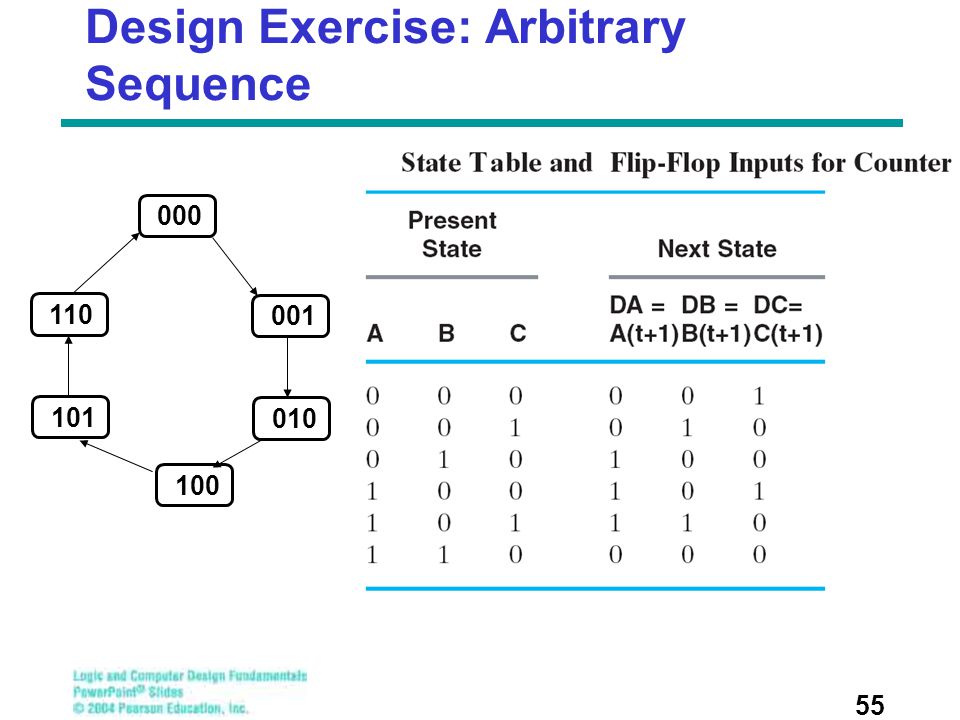
56
Arbitrary Count sequence: next state equation
3 Flip-flops required Find the next state equations: DC, DB, DA. A B C DA x 1 Be careful with Table sequence x 0 A B C DC x 0 A B C DB x 0 DA = A’B+AB’ = AB DB = C DC = B’C’

57
Counter schematic DA = A’B+AB’ = AB DB = C DC = B’C’
What about unused states? Complete the state diagram

Similar presentations


 contains datapath unit and control unit. Datapath: A.>")
 Terms of Use Chapter 7 – Registers.>")


