Download presentation
Presentation is loading. Please wait.

1
Commande d’actionneurs à l’aide d’un microprocesseur
1 Prise en main du DSP Christian Koechli

2
Composants de l’électronique de commande
CPU: DSP ou mcontrôleur Signaux de mesure Mesure Capteurs Signaux logiques Driver Alim. de la « logique » Signaux de commande Alim puissance

3
Texas Instruments TMS320F28069
Processeur 32 bits Architecture Harvard F=90MHz (80 protos) FPU / CLA 256 kB flash 100 kB RAM 1 AD (16 canaux 12 bits 3MSps) SPI/I2C/CAN/USB 2 RS232 54 GPIO 3 CAPTURE +4 HRCap+ 2eQep 8 ePWM
 FPU / CLA. 256 kB flash. 100 kB RAM. 1 AD (16 canaux 12 bits 3MSps) SPI/I2C/CAN/USB. 2 RS GPIO. 3 CAPTURE +4 HRCap+ 2eQep. 8 ePWM.")
4
F28069 Block Diagram

5
Memory Map

6
Gestion de la mémoire

7
Watchdog Timer

8
General Purpose IO

9
GPIO Multiplexing

12
Exemple de programmation
extern volatile struct GPIO_CTRL_REGS GpioCtrlRegs; extern volatile struct GPIO_DATA_REGS GpioDataRegs; struct GPIO_CTRL_REGS { union GPACTRL_REG GPACTRL; // GPIO A Control Register (GPIO0 to 31) union GPA1_REG GPAQSEL1; // GPIO A Qualifier Select 1 Register (GPIO0 to 15) union GPA2_REG GPAQSEL2; // GPIO A Qualifier Select 2 Register (GPIO16 to 31) union GPA1_REG GPAMUX1; // GPIO A Mux 1 Register (GPIO0 to 15) union GPA2_REG GPAMUX2; // GPIO A Mux 2 Register (GPIO16 to 31) union GPADAT_REG GPADIR; // GPIO A Direction Register (GPIO0 to 31) union GPADAT_REG GPAPUD; // GPIO A Pull Up Disable Register (GPIO0 to 31) Uint rsvd1; // reserved union GPBCTRL_REG GPBCTRL; // GPIO B Control Register (GPIO32 to 63) union GPB1_REG GPBQSEL1; // GPIO B Qualifier Select 1 Register (GPIO32 to 47) union GPB2_REG GPBQSEL2; // GPIO B Qualifier Select 2 Register (GPIO48 to 63) union GPB1_REG GPBMUX1; // GPIO B Mux 1 Register (GPIO32 to 47) union GPB2_REG GPBMUX2; // GPIO B Mux 2 Register (GPIO48 to 63) union GPBDAT_REG GPBDIR; // GPIO B Direction Register (GPIO32 to 63) union GPBPUD_REG GPBPUD; // GPIO B Pull Up Disable Register (GPIO32 to 63) Uint rsvd2[24];// reserved union AIO_REG AIOMUX1; // Analog IO Mux 1 Register (AIO0 to 15) Uint rsvd3; // reserved union AIODAT_REG AIODIR; // Analog IO Direction Register (AIO0 to 15) Uint rsvd4[5]; // reserved };
 union GPA1_REG GPAQSEL1; // GPIO A Qualifier Select 1 Register (GPIO0 to 15) union GPA2_REG GPAQSEL2; // GPIO A Qualifier Select 2 Register (GPIO16 to 31) union GPA1_REG GPAMUX1; // GPIO A Mux 1 Register (GPIO0 to 15) union GPA2_REG GPAMUX2; // GPIO A Mux 2 Register (GPIO16 to 31) union GPADAT_REG GPADIR; // GPIO A Direction Register (GPIO0 to 31) union GPADAT_REG GPAPUD; // GPIO A Pull Up Disable Register (GPIO0 to 31) Uint32 rsvd1; // reserved. union GPBCTRL_REG GPBCTRL; // GPIO B Control Register (GPIO32 to 63) union GPB1_REG GPBQSEL1; // GPIO B Qualifier Select 1 Register (GPIO32 to 47) union GPB2_REG GPBQSEL2; // GPIO B Qualifier Select 2 Register (GPIO48 to 63) union GPB1_REG GPBMUX1; // GPIO B Mux 1 Register (GPIO32 to 47) union GPB2_REG GPBMUX2; // GPIO B Mux 2 Register (GPIO48 to 63) union GPBDAT_REG GPBDIR; // GPIO B Direction Register (GPIO32 to 63) union GPBPUD_REG GPBPUD; // GPIO B Pull Up Disable Register (GPIO32 to 63) Uint16 rsvd2[24];// reserved. union AIO_REG AIOMUX1; // Analog IO Mux 1 Register (AIO0 to 15) Uint32 rsvd3; // reserved. union AIODAT_REG AIODIR; // Analog IO Direction Register (AIO0 to 15) Uint16 rsvd4[5]; // reserved. };")
13
Exemple de programmation
struct GPIO_DATA_REGS { union GPADAT_REG GPADAT; // GPIO Data Register (GPIO0 to 31) union GPADAT_REG GPASET; // GPIO Data Set Register (GPIO0 to 31) union GPADAT_REG GPACLEAR; // GPIO Data Clear Register (GPIO0 to 31) union GPADAT_REG GPATOGGLE; // GPIO Data Toggle Register (GPIO0 to 31) union GPBPUD_REG GPBDAT; // GPIO Data Register (GPIO32 to 63) union GPBDAT_REG GPBSET; // GPIO Data Set Register (GPIO32 to 63) union GPBDAT_REG GPBCLEAR; // GPIO Data Clear Register (GPIO32 to 63) union GPBDAT_REG GPBTOGGLE; // GPIO Data Toggle Register (GPIO32to 63) Uint rsvd1[8]; // reserved union AIODAT_REG AIODAT; // Analog IO Data Register (AIO0-15) Uint rsvd2; union AIODAT_REG AIOSET; // Analog IO Data Set Register (AIO0-15) Uint rsvd3; union AIODAT_REG AIOCLEAR; // Analog IO Data Clear Register (AIO0-15) Uint rsvd4; union AIODAT_REG AIOTOGGLE; // Analog IO Data Toggle Register (AIO0-15) Uint rsvd5; }; Au reset toutes les pates sont configurées comme IO/input. Pour configurer la patte EPWM1A comme périphérique EPWM : EALLOW; GpioCtrlRegs.GPAMUX1.bit.GPIO0=1 ; EDIS;
 union GPADAT_REG GPASET; // GPIO Data Set Register (GPIO0 to 31) union GPADAT_REG GPACLEAR; // GPIO Data Clear Register (GPIO0 to 31) union GPADAT_REG GPATOGGLE; // GPIO Data Toggle Register (GPIO0 to 31) union GPBPUD_REG GPBDAT; // GPIO Data Register (GPIO32 to 63) union GPBDAT_REG GPBSET; // GPIO Data Set Register (GPIO32 to 63) union GPBDAT_REG GPBCLEAR; // GPIO Data Clear Register (GPIO32 to 63) union GPBDAT_REG GPBTOGGLE; // GPIO Data Toggle Register (GPIO32to 63) Uint16 rsvd1[8]; // reserved. union AIODAT_REG AIODAT; // Analog IO Data Register (AIO0-15) Uint16 rsvd2; union AIODAT_REG AIOSET; // Analog IO Data Set Register (AIO0-15) Uint16 rsvd3; union AIODAT_REG AIOCLEAR; // Analog IO Data Clear Register (AIO0-15) Uint16 rsvd4; union AIODAT_REG AIOTOGGLE; // Analog IO Data Toggle Register (AIO0-15) Uint16 rsvd5; }; Au reset toutes les pates sont configurées comme IO/input. Pour configurer la patte EPWM1A comme périphérique EPWM : EALLOW; GpioCtrlRegs.GPAMUX1.bit.GPIO0=1 ; EDIS;")
14
Interrupts

15
Maskable Interrupt Processing Conceptual Core Overview
1 (IFR) “Latch” INT1 INT2 INT14 Core Interrupt C28x Core (INTM) “Global Switch” (IER) “Switch” A valid signal on a specific interrupt line causes the latch to display a “1” in the appropriate bit If the individual and global switches are turned “on” the interrupt reaches the core
 Latch INT1. INT2. INT14. Core. Interrupt. C28x. Core. (INTM) Global Switch (IER) Switch A valid signal on a specific interrupt line causes the latch to display a 1 in the appropriate bit. If the individual and global switches are turned on the interrupt reaches the core.")
16
Interrupt Flag Register (IFR)
RTOSINT DLOGINT INT14 INT13 INT12 INT11 INT10 INT9 8 9 10 11 12 13 14 15 INT8 INT7 INT6 INT5 INT4 INT3 INT2 INT1 1 2 3 4 5 6 7 Pending : IFR Bit = 1 Absent : IFR Bit = 0 /*** Manual setting/clearing IFR ***/ extern cregister volatile unsigned int IFR; IFR |= 0x0008; //set INT4 in IFR IFR &= 0xFFF7; //clear INT4 in IFR Compiler generates atomic instructions (non-interruptible) for setting/clearing IFR If interrupt occurs when writing IFR, interrupt has priority IFR(bit) cleared when interrupt is acknowledged by CPU Register cleared on reset
 for setting/clearing IFR. If interrupt occurs when writing IFR, interrupt has priority. IFR(bit) cleared when interrupt is acknowledged by CPU. Register cleared on reset.")
17
Interrupt Enable Register (IER)
RTOSINT DLOGINT INT14 INT13 INT12 INT11 INT10 INT9 8 9 10 11 12 13 14 15 INT8 INT7 INT6 INT5 INT4 INT3 INT2 INT1 1 2 3 4 5 6 7 Enable: Set IER Bit = 1 Disable: Clear IER Bit = 0 /*** Interrupt Enable Register ***/ extern cregister volatile unsigned int IER; IER |= 0x0008; //enable INT4 in IER IER &= 0xFFF7; //disable INT4 in IER Compiler generates atomic instructions (non-interruptible) for setting/clearing IER Register cleared on reset
 for setting/clearing IER. Register cleared on reset.")
18
Interrupt Global Mask Bit
INTM ST1 Bit 0 INTM used to globally enable/disable interrupts: Enable: INTM = 0 Disable: INTM = 1 (reset value) INTM modified from assembly code only: /*** Global Interrupts ***/ asm(“ CLRC INTM”); //enable global interrupts asm(“ SETC INTM”); //disable global interrupts
 INTM modified from assembly code only: /*** Global Interrupts ***/ asm( CLRC INTM ); //enable global interrupts. asm( SETC INTM ); //disable global interrupts.")
19
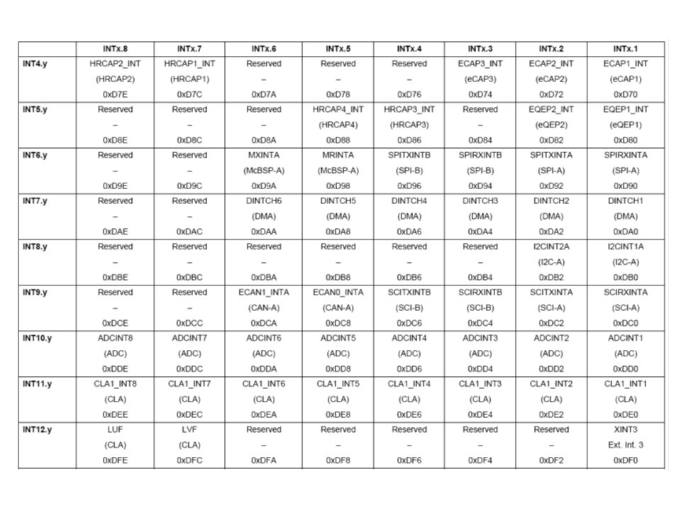
F28069 PIE Interrupt Assignment Table

21
Déroulement d’un appel d’interruption

Similar presentations


>")


 – processor continually checks IO device to see if it is ready for data transfer –Inefficient,>")

