Download presentation
Presentation is loading. Please wait.

1
Timer modules in PIC 16F877

2
The PIC 16F877 basically has three independent timer modules, denoted by the symbols, TIMER-0, TIMER1,andTIMER2. . These timer module terminals are also multiplexed with other functions for handling alternate functions.

3
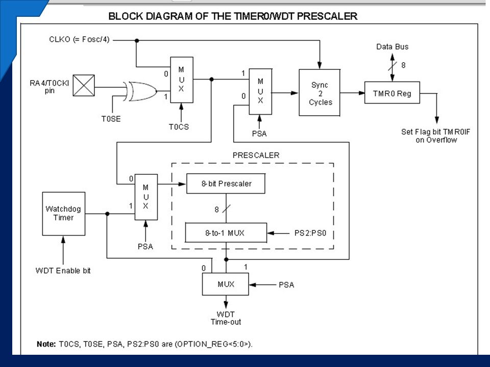
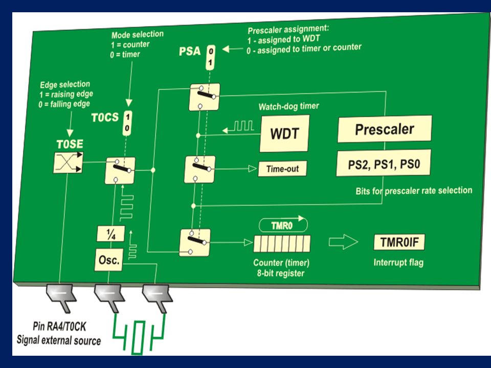
TIMER-0 module Timer-0 module has built in 8 bit timer/counter It is easily readable/writable Easily select internal/external clock pulses Edge selection for external clock pulse Built in 8 bit software programmable pre-scalar functions((shared with Watchdog timer) Interrupt with overflow from the value FFh to 00h
 Interrupt with overflow from the value FFh to 00h")
5
The Timer0 module has a dedicated 8bit register that can be accessed for read and write operations. This register can be accessed from BANK 0 and BANK 2, and is named " TMR0 ". A direct read (MOVf TMR0,w) will transfer the value of the Timer0 counter directly to the W register, while a direct write (MOVwf, TMR0) will transfer the content of the W register to the Timer0 counter.. “TMR0 ”.
 will transfer the value of the Timer0 counter directly to the W register, while a direct write (MOVwf, TMR0) will transfer the content of the W register to the Timer0 counter.. TMR0 ..")
10
The main registers associated with timer 0 module are

11
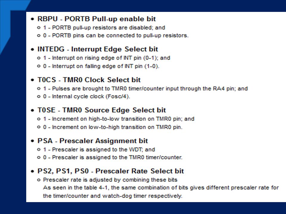
OPTION_REG register…… The operation of the Timer0 module can be determined by specific bits of the OPTION_REG register

12
OPTION_REG register BIT (T0CS): This is the "TMR0 Clock Source Select bit". The value of this bit will determine if the TMR0 register will be increased on every internal instruction cycle of the PIC (in other words once every 4 clock pulses) or on every pulse on the TOCKI pin input. The possible values for the TOCS bit are: 0: The increment is done on every internal instruction cycle 1: The increament is done on every pulse on the TOCKI pin input of the PIC
 or on every pulse on the TOCKI pin input. The possible values for the TOCS bit are: 0: The increment is done on every internal instruction cycle 1: The increament is done on every pulse on the TOCKI pin input of the PIC.")
13
OPTION_REG register BIT (T0SE): This is the "TMR0 Source Edge Select bit". This bit has an effect only if the T0CS bit (above) is 1, in other words if the TMR0 register increases with external pulses on the TOCKI pin. The increament is done at the EDGE of each pulse. The value of the TOSE bit will determine if the increment will be done on the POSITIVE GOING transition, or on the NEGATIVE GOING transition of the pulse. The values that this bit can get are : 0: The increment is done on the LOW to HIGH transition of the pulse 1: The increament is done on the HIGH to LOW transition of the pulse
 is 1, in other words if the TMR0 register increases with external pulses on the TOCKI pin. The increament is done at the EDGE of each pulse. The value of the TOSE bit will determine if the increment will be done on the POSITIVE GOING transition, or on the NEGATIVE GOING transition of the pulse. The values that this bit can get are : 0: The increment is done on the LOW to HIGH transition of the pulse 1: The increament is done on the HIGH to LOW transition of the pulse.")
14
Prescaler Assignment bit(PSA) This is the "Prescaler Assignment bit". The prescaler is another module of the PIC. The prescaler divides the input counts before they arrive at the TMR0 register. The prescaler can divide both the pulses from the TOCKI pin (when TOCS=1) as well as the counts from the internal instruction cycles (when TOCS-0). The PSA bit can have the following values: 0: The PSA is assigned to the Timer0 module and the counts are divided before they reach the TMR0 register 1: The PSA is assigned to the Watchdog timer (another module of the PIC) and the counts will arrive directly to the TMR0 register
 as well as the counts from the internal instruction cycles (when TOCS-0). The PSA bit can have the following values: 0: The PSA is assigned to the Timer0 module and the counts are divided before they reach the TMR0 register 1: The PSA is assigned to the Watchdog timer (another module of the PIC) and the counts will arrive directly to the TMR0 register.")
15
The function of the PSA bit 0

16
The function of the PSA bit 1

17
NB: When the prescaler is assigned to the timer/counter, any write to the TMR0 register will clear the prescaler; When the prescaler is assigned to watch-dog timer, a CLRWDT instruction will clear both the prescaler and WDT;

18
OPTION_REG register BIT (PS): These 3 bits are the "Prescaler Rate Select bits". These bits have an effect on the prescaler division rate all the time, but they have an effect, ONLY if the prescaler is assigned to the Timer0 module (when PSA=0). ie, If the prescaler is assigned to the Timer0 module, then these 3 bits will determine the division rate. If for example the division rate is 64, then the TMR0 module will increase it's value by one, after 64 counts.
. ie, If the prescaler is assigned to the Timer0 module, then these 3 bits will determine the division rate. If for example the division rate is 64, then the TMR0 module will increase it s value by one, after 64 counts..")
19
000: 1/2 division 001: 1/4 division 010: 1/8 division 011: 1/16 division 100: 1/32 division 101: 1/64 division 110: 1/128 division 111: 1/256 division

20
The Timer0 Interrupt. TMR0 interrupt is activated only when the TMR0 register overflows from the value FFh to 00h. This overflow sets bit TMR0IF

21
The TMR0IE interrupt can be controlled by the INTCON register bit 5 (TMR0IE - TMR0 Interrupt Enabled). When the TMR0 Interrupt is raised, the INTCON bit 2 (TMR0IF - TMR0 Interrupt Flag) is raised to indicate that the TMR0 interrupt is occurred. The TMR0IF must be cleared in software,by (BCF INTCON, TMR0IF) for the TMR0 interrupt to be re-enabled.
 is raised to indicate that the TMR0 interrupt is occurred. The TMR0IF must be cleared in software,by (BCF INTCON, TMR0IF) for the TMR0 interrupt to be re-enabled..")
22
Timer-0 Interrupt The interrupt can be masked by clearing bit TMR0IE. Bit TMR0IF must be cleared in software by the Timer 0 module Interrupt Service Routine before re-enabling this interrupt. The TMR0 interrupt cannot awaken the Processor from Sleep since the timer is shut-off during Sleep.

23
NOTES: Setting Timer0: Timer mode is selected by the T0CS bit of the OPTION_REG register, (T0CS: 0=timer, 1=counter); When used, the prescaler should be assigned to the timer/counter by clearing the PSA bit of the OPTION_REG register. The prescaler rate is set by using the PS2-PS0 bits of the same register; and When using interrupt, the GIE and TMR0IE bits of the INTCON register should be set.

24
NOTES… To measure time: Reset the TMR0 register or write some decided value to it; Elapsed time (in microseconds when using quartz 4MHz) is measured by reading the TMR0 register; and The flag bit TMR0IF of the INTCON register is automatically set every time the TMR0 register overflows. If enabled, an interrupt occurs.

25
Notes….. To count pulses: The polarity of pulses are to be counted is selected on the RA4 pin are selected by the TOSE bit of the OPTION register (T0SE: 0=positive, 1=negative pulses); and Number of pulses may be read from the TMR0 register. The prescaler and interrupt are used in the same manner as in timer mode.
; and Number of pulses may be read from the TMR0 register. The prescaler and interrupt are used in the same manner as in timer mode..")
26
TIMER 1

27
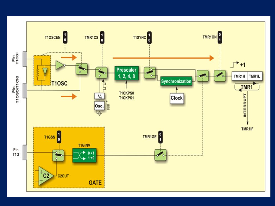
16-bit length timer/counter. It can operate as a Timer, or as a synchronous/asynchronous counter. To set-up and control the Timer1 module, there is a dedicated control register named T1CON

28
T1OSCEN - LP Oscillator Enable Control bit 1 - LP oscillator is enabled for timer TMR1 clock (oscillator with low power consumption and frequency 32.768 kHz); and 0 - LP oscillator is off. T1SYNC - Timer1 External Clock Input Synchronization Control bit enables synchronization of the LP oscillator input or T1CKI pin input with the microcontroller internal clock. When counting pulses from the local clock source (bit TMR1CS = 0), this bit is ignored. 1 - Do not synchronize external clock input; and 0 - Synchronize external clock input. TMR1CS - Timer TMR1 Clock Source Select bit 1 - Counts pulses on the T1CKI pin (on the rising edge 0-1); and 0 - Counts pulses of the internal clock of microcontroller. TMR1ON - Timer1 On bit 1 - Enables Timer TMR1; and 0 - Stops Timer TMR1.
, this bit is ignored. 1 - Do not synchronize external clock input; and 0 - Synchronize external clock input. TMR1CS - Timer TMR1 Clock Source Select bit 1 - Counts pulses on the T1CKI pin (on the rising edge 0-1); and 0 - Counts pulses of the internal clock of microcontroller. TMR1ON - Timer1 On bit 1 - Enables Timer TMR1; and 0 - Stops Timer TMR1..")
31
Timer1…... Timer TMR1 Oscillator RC0/T1OSO and RC1/T1OSI pins are used to register pulses coming from peripheral electronics, Timer TMR1 Gate Timer 1 gate source is software configurable,to be the T1G pin or the output of comparator C2. This gate allows the timer to directly time external events using the logic state on the T1G pin or analog events using the comparator C2 output. Refer to figure above. In order to time a signals duration it is sufficient to enable such gate and count pulses having passed through it. Timer TMR1 Prescaler Timer TMR1 has a completely separate prescaler which allows 1, 2, 4 or 8 divisions of the clock input. The prescaler is not directly readable or writable. However, the prescaler counter is automatically cleared upon write to the TMR1H or TMR1L register

32
Timer 1 operates in two different modes. They are 1) Timer mode 2) Counter mode Timer 1 pin can be enabled/disabled easily by setting/clearing the control bit (TMR1ON). The operating mode of timer 1 module is selected by using the clock select bit (TMR1CS), in timer mode. The timer 1 increases on every machine cycle But in counter mode, it increases on every rising edge of the external clock input.
 Timer mode 2) Counter mode Timer 1 pin can be enabled/disabled easily by setting/clearing the control bit (TMR1ON). The operating mode of timer 1 module is selected by using the clock select bit (TMR1CS), in timer mode. The timer 1 increases on every machine cycle But in counter mode, it increases on every rising edge of the external clock input..")
33
Timer 1 Operation in Timer Mode The Timer mode can be easily selected by clearing the TMR1CS bit. In this mode, the input clock to the timer is FOSC/4. The synchronize control bit, T1SYNC, has no effect since the internal clock is always in sync. Timer1 Operation in harmonized

34
Timer mode

35
Counter Mode The Counter mode is selected by setting timer 1 TIMER/counter select bit (TMR1CS=1). In this mode, the timer increments on every rising edge of clock input on pin RC1/T1OSI/CCP2 when bit T1OSCEN is set, or on pin RC0/T1OSO/T1CKI when bit T1OSCEN is cleared.

36
Counter Mode….

37
SYNCHRONOUS COUNTER TMR1 in counter mode Timer TMR1 starts to operate as a counter by setting the TMR1CS bit. It means that the timer TMR1 is incremented on the rising edge of the external clock input T1CKI. If control bit T1SYNC of the T1CON register is cleared, the external clock inputs will be synchronized on their way to the TMR1 register. In other words, the timer TMR1 is synchronized to the microcontroller system clock and called a synchronous counter.

39
Timer1_ Asynchronous Counter Mode If control bit T1SYNC (T1CON ) is set, the external clock input is not synchronized. The timer continues to increment asynchronous to the internal phase clocks. The timer will continue to run during Sleep and can generate an interrupt-on-overflow which will wake-up the processor. However, special precautions in software are needed to read/write the timer. In Asynchronous Counter mode, Timer 1 cannot be used as a time base for capture or compare operations

40
Register memory organization for timer 1 timer/counter module

41
TIMER 2

42
TMR 2 Module(PWM UNIT)
")
43
TMR2

44
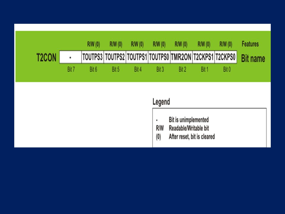
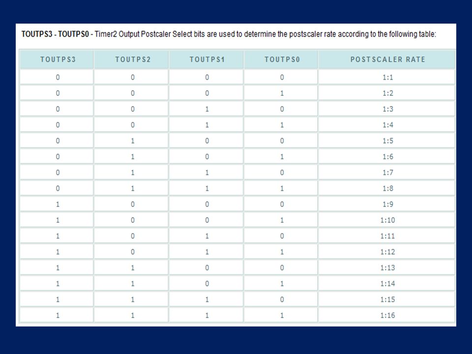
TIMER2 The pulses from the quartz oscillator first pass through the prescaler whose rate may be changed by combining the T2CKPS1 and T2CKPS0 bits. The output of the prescaler is then used to increment the TMR2 register starting from 00h. The values of TMR2 and PR2 are constantly compared and the TMR2 register keeps on being incremented until it matches the value in PR2. When a match occurs, the TMR2 register is automatically cleared to 00h. The timer TMR2 Postscaler is incremented and its output is used to generate an interrupt if it is enabled.

45
The TMR2 and PR2 registers are both fully readable and writable. Counting may be stopped by clearing the TMR2ON bit, which contributes to power saving. As a special option, the moment of TMR2 reset may be also used to determine synchronous serial communication baud rate. The timer TMR2 is controlled by several bits of the T2CON register.

49
Register memory organization of timer 2 module

50
Upon power-on, the PR2 register contains the value FFh; Both prescaler and postscaler are cleared by writing to the TMR2 register; Both prescaler and postscaler are cleared by writing to the T2CON register; and On any reset, both prescaler and postscaler are cleared. NB:

Similar presentations


.>")
>")


 is a peripheral which allows the user to time and control different events. Capture Mode provides.>")
