Download presentation
Presentation is loading. Please wait.

1
ECE 333 Linear Electronics
Chapter Bipolar Junction Transistors (BJTs) Physical structure of BJT I-V Characteristics circuits based on BJTs Compared with MOSFETs
 Physical structure of BJT I-V Characteristics circuits based on BJTs. Compared with MOSFETs.")
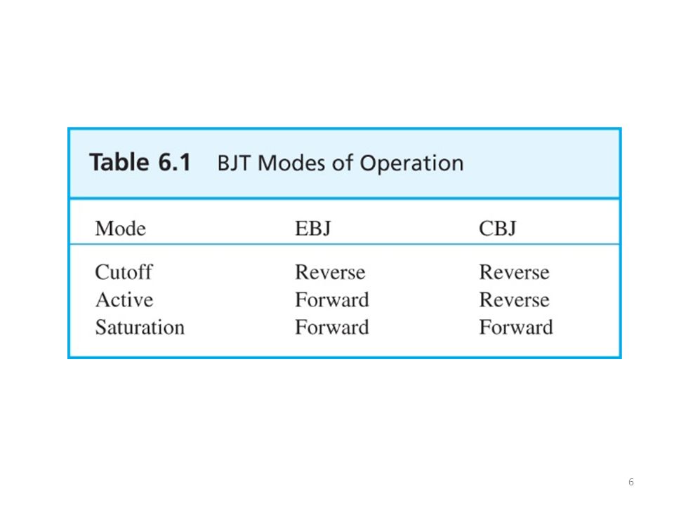
2
Introduction The invention of BJT (page 305)
(Bardeen, Shockley and 1948 in Brattain’s lab)
")
3
Story behind the First BJT
Bardeen was a quantum physicist, Brattain a gifted experimenter in materials science, and Shockley, the leader of their team, was an expert in solid-state physics. 1947: W. Brattain and J. Bardeen (Bell Labs) experimentally demonstrated the device J. Pierce (Bell Labs) name the device: transfer + resistor = transistor 1949: W. Shockley theoretically described bipolar junction transistor 1956: Nobel Prize
 experimentally demonstrated the device J. Pierce (Bell Labs) name the device: transfer + resistor = transistor 1949: W. Shockley theoretically described bipolar junction transistor 1956: Nobel Prize")
4
6.1 Device Structure and Physical Operation
6.1.1 Figure 6.1 A simplified structure of the npn transistor.

5
Figure 6.2 A simplified structure of the pnp transistor.

7
6.1.2 Operation of the npn Transistor in the Active Mode
Figure 6.3 Current flow in an npn transistor biased to operate in the active mode. (Reverse current components due to drift of thermally generated minority carriers are not shown.)
")
8
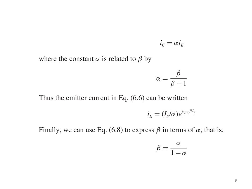
Collector current Base current Emitter current
VT : the thermal potential β is common-emitter current gain

10
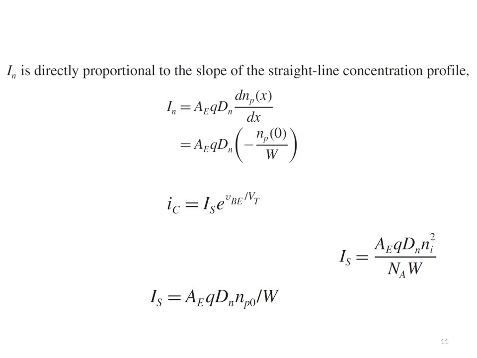
Minority-Carrier Distribution

12
Equivalent Circuit Models

13
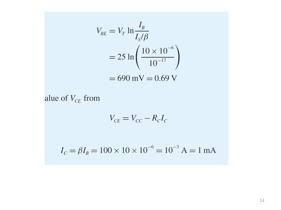
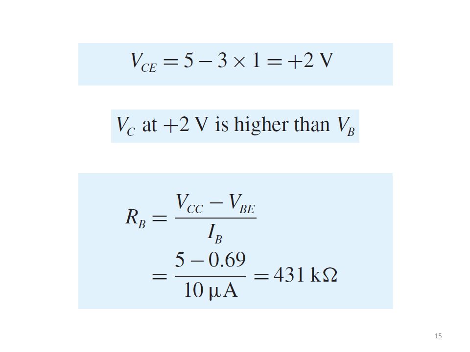
Example 6.1

16
6.1.3 Structure of Actual BJTs
Most Si BJT are designed so that recombination of injected electrons in the base-emitter space charge region is smaller than the other components. Figure 6.7 Cross section of an npn BJT.

17
The high performance BJT
Use different materials in emitter and base To increase βF , we need to increase ______ and decrease _______ 𝛽 𝐹 = 𝐷 𝐵 𝑊 𝐸 𝑁 𝐸 𝑛 2 𝑖𝐵 𝐷 𝐸 𝑊 𝐵 𝑁 𝐵 𝑛 2 𝑖𝐸

18
6.1.4 Operation in the saturation mode
Different with that in MOSFETs

19
Figure 6.9 Modeling the operation of an npn transistor in saturation by augmenting the model of Fig. 6.5(c) with a forward- conducting diode DC. Note that the current through DC increases iB and reduces iC.
 with a forward- conducting diode DC. Note that the current through DC increases iB and reduces iC..")
20
6.1.5 The pnp Transistor Figure 6.10 Current flow in a pnp transistor biased to operate in the active mode.

21
6.2 Current-Voltage Characteristics
6.2.1 Circuit Symbols and Conventions Figure 6.12 Circuit symbols for BJTs.

22
Figure 6.13 Voltage polarities and current flow in transistors operating in the active mode.

24
Example 6.2

27
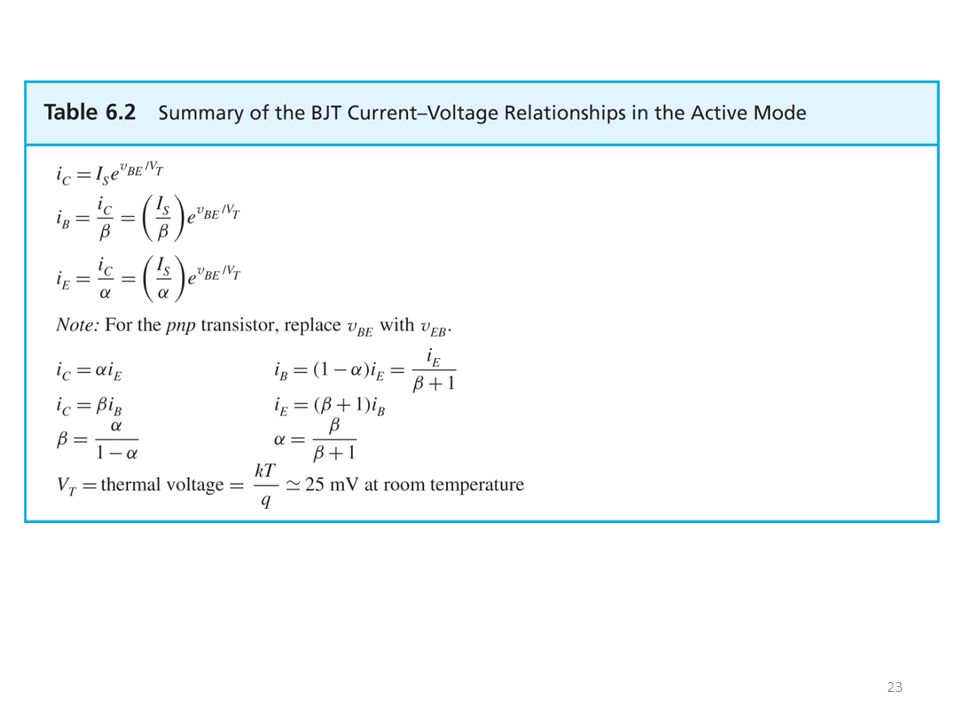
6.2.2 Graphical representation of transistor characteristics
1/VT ≈ 40, the i-v curves are sharp 𝑖 𝐸 = 𝐼 𝑆 𝛼 𝑒 𝑣 𝐵𝐸 / 𝑉 𝑇 𝑖 𝐵 = 𝐼 𝑆 𝛽 𝑒 𝑣 𝐵𝐸 / 𝑉 𝑇 𝑖 𝐶 = 𝐼 𝑆 𝑒 𝑣 𝐵𝐸 / 𝑉 𝑇 Different with MOSFET

28
Exercise 6.15

29
6.2.3 Dependence of iC on the Collector Voltage – The Early Effect
What is Early Effect (or base-width modulation effect)?
")
30
6.2.3 Dependence of iC on the Collector Voltage – The Early Effect
The current including Early Effect Output resistance (not infinite)
")
31
6.2.3 Dependence of iC on the Collector Voltage – The Early Effect
The equivalent circuit taking into account of Early Effect Figure 6.19 Large-signal, equivalent-circuit models of an npn BJT operating in the active mode in the common-emitter configuration with the output resistance ro included.

32
6.2.4 An Alternative Form of the Common-Emitter Characteristics
The Common-Emitter Current Gain β

33
6.2.4 An Alternative Form of the Common-Emitter Characteristics
The Saturation Voltage VCEsat and Saturation Resistance RCEsat In comparison with MOSFET Linear resistance βforced

34
6.2.4 An Alternative Form of the Common-Emitter Characteristics
A simplified equivalent-circuit model of the saturated transistor

35
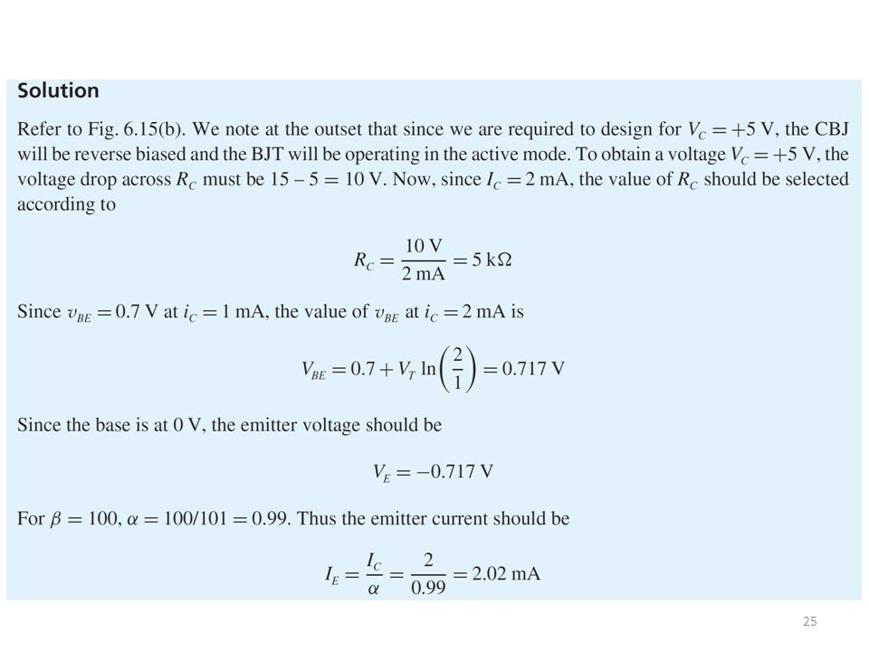
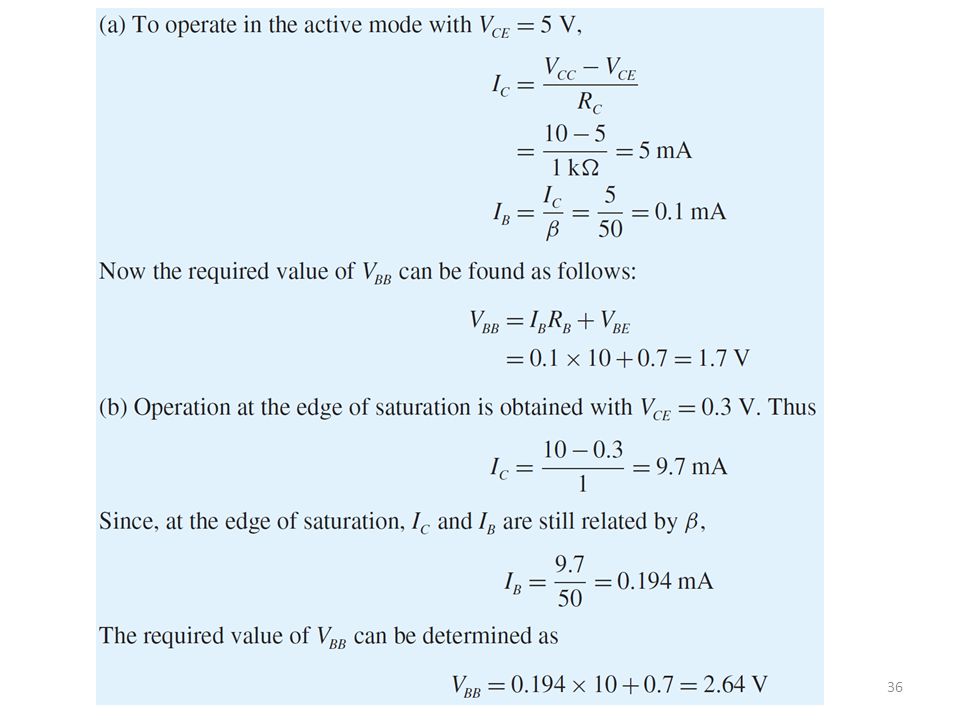
Example 6.3 For the circuit in Fig. 6.22, it is required to determine VBB that results in the transistor operating In active mode with VCE=5V At the edge of saturation Deep in saturation with βforced=10 (VBE remains constant at 0.7V and β=50) Solve: (analysis: active mode VBE is Forward biased VCE is known VC is known IC can be calculated IB can be Calculated VBB = …
 Solve: (analysis: active mode VBE is. Forward biased. VCE is known VC is known IC can be calculated IB can be. Calculated VBB = …")
37
Saturation mode of operation

38
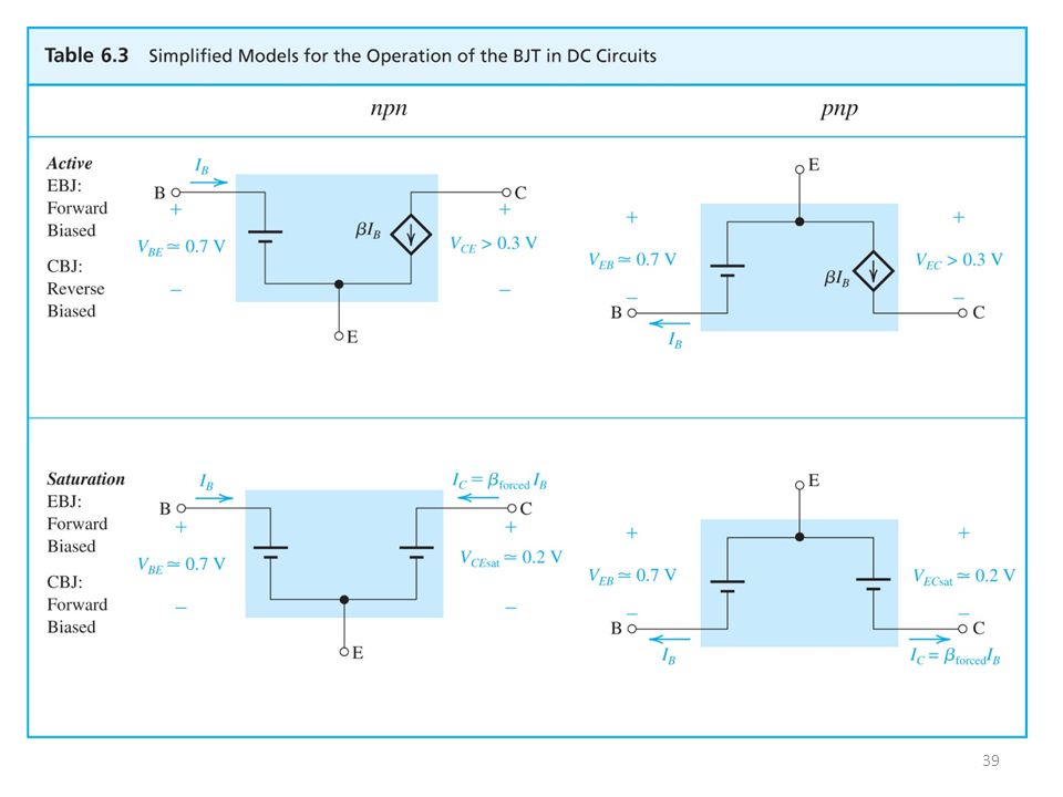
6.3 BJT Circuit at DC Use simple model: |VBE|=0.7V for a conducting transistor and |VCE|=0.2V for a saturated transistor Accurate model will increase complexity and impede insight in design SPICE simulation in the final stage of design

40
A note on Units: a consistent set of units:
volts (V), milliamps (mA), and kilohms (kΩ) Example 6.4: β=100. determine all node voltages and branch currents for the following circuit.
, milliamps (mA), and kilohms (kΩ) Example 6.4: β=100. determine all node voltages and branch currents for the following circuit.")
41
Use a simple model: from a simple analysis we know that the transistor is conducting, so VBE=0.7 V. This is the first step Double-Check: the transistor is in active mode, saturation mode or cut-off mode?

42
Example 6.5: β>50 for the following circuit
Assume active-mode

43
Example 6.5 (continue…) βforced = IC / IB = 1.5 saturation mode
Assume Saturation-mode βforced = IC / IB = 1.5 saturation mode

44
Example 6.6 Cutoff mode

45
Example 6.7 analyze all node voltages and branch currents
pnp Since no β is not given, we can assume β=100

46
Example 6.8: β=100, determine all node voltages and currents
Assume active-mode Is this design good or bad? What if β were 10% higher? If β = 110, IC = 4.73 mA VC=10-2×4.73=0.54V saturation

47
Example 6.9: the minimum β is 30
Either active or saturation mode: First assume active mode IB=0 VB=0 VE=0.7IE=4.3 mA. However, IC is limited at 5/10k = 0.5 mA saturation

48
Yes! saturated

49
6.4 Transistor Breakdown and Temperature Effects
CBJ breakdown is usually not destructive, at BVCBO>=50V EBJ breakdown usually in an avalanche manner at BVEBO=6~8V, destructive, with β permanently reduced

50
Figure 6.32 The BJT common-base characteristics including the transistor breakdown region.

51
Figure 6.33 The BJT common-emitter characteristics including the breakdown region.

52
6.4.2 Dependence of β on IC and Temperature
Figure 6.34 Typical dependence of β on IC and on temperature in an integrated-circuit npn silicon transistor intended for operation around 1 mA.

Similar presentations


>")

 NPNPNP.>")
 Dr. Wojciech Jadwisienczak EE314.>")


 Chapter #6: Bipolar Junction Transistors from.>")


 – PNP transistor (structure, operation, models) BJT Amplifiers –>")
>")
 1.>")
