Download presentation
Presentation is loading. Please wait.

1
How to use ISE Dept. of Info & Comm. Eng. Prof. Jongbok Lee

2
A. Introduction Xilinx ISE (Integrated Software Environment) –VHDL/Verilog coding –Synthesis –FPGA Programming & Implementation
 –VHDL/Verilog coding –Synthesis –FPGA Programming & Implementation.")
3
I. Start Double click Xilinx ISE 10.1i –Project Navigator appears File New Project New Project window –Project Name : proj_name –Top-Level Module Type : HDL –Click [next] –File ***.ise is created

4
New Project window –Device Family : Spartan3 –Device : xc3s400 –Package : FT256 –Speed Grade : -4 –[next][next][finish]
![New Project window –Device Family : Spartan3 –Device : xc3s400 –Package : FT256 –Speed Grade : -4 –[next][next][finish]](http://images.slideplayer.com/37/10723698/slides/slide_4.jpg "New Project window –Device Family : Spartan3 –Device : xc3s400 –Package : FT256 –Speed Grade : -4 –[next][next][finish]")
5
II. VHDL Coding Project New Source –Select VHDL Module –File Name : myinv Project Add Source –You can add an existing vhdl source Define VHDL Source window –Port Name : Direction –a: in –b: out –[next][finish]

6
–if VHDL window appears, File Save Source window : Source for Synthesis/Implementation –You can double click Check Syntax and find the syntax error Architecture Behavioral of myinv is begin b <= not(a); end Behavioral
; end Behavioral")
7
IV. Synthesis Source window : select Synthesis/Implementation –Synthesize-XST click Check Syntax if wrong, see the View Synthesis Report and fix it. if right Save FPGA pin number assigment –Source window: select myinv.vhd –Process window: User Constraints Floor Plan IO - Pre Synthesis Xilinx PACE window appears Design Object List-I/O Pins –I/O Name : I/O Direction : Loc –a : Input :G3 –b : Output :A12 File Save

8
Note –In one project, only one module can be synthesized. –if the User Constraint, Synthesize- XST,Implement, Generate menu does not appear in the process window, select module, click right mouse button and select to execute Set As Top Module –Then the three triangle appears in front of the module.

9
Implementation –Translate : transform the netlist into the inner format –Map : optimize and then map the logic circuits to the FPGA resources such as CLB and IOB. –Place & Route : connect the gates allocated in CLBs

10
note –CLB(Configurable Logic Block) consists of 3 LUTs(Look Up Table) and 2 Flip Flops the basic block that constitutes FPGA
 consists of 3 LUTs(Look Up Table) and 2 Flip Flops the basic block that constitutes FPGA")
11
Synthesize and P&R –Process window : double click Synthesize- XST –Process window : double click Implement Design

12
EDA-Lab II Experiment Kit Function : An equipment for the verification of FPGA circuit design Usage : education, circuit development FPGA capacity : 400,000 gates Supporting software : Design Pro Shop

14
V. Emulation Emulation ? –a hardware mimics another hardware How to set up –connect EDA-Lab 2’s Xilinx USB JTAG port to PC. –connect main board’s Jumper pin and targer FPGA’s Expansion Port by cable (JP6.0~CN1.17). –Turn on the Power. –The cable colors should be matched in correspondence.
. –Turn on the Power. –The cable colors should be matched in correspondence..")
15
Generating an FPGA programming file –Process window : Double click Generate Programming File See the Programming File Generation Report –make sure myinv.bit has been created. –It should be in the project folder.

16
iMPACT Process window –Configure Target Device Manage Configuration Project(iMPACT) –File Initialize Chain –Assign New Configuration File : myinv.bit [open] –[bypass] –select xc3s400 and click the right mouse button program : Program Succeeded !
![iMPACT Process window –Configure Target Device Manage Configuration Project(iMPACT) –File Initialize Chain –Assign New Configuration File : myinv.bit [open] –[bypass] –select xc3s400 and click the right mouse button program : Program Succeeded !](http://images.slideplayer.com/37/10723698/slides/slide_16.jpg "iMPACT Process window –Configure Target Device Manage Configuration Project(iMPACT) –File Initialize Chain –Assign New Configuration File : myinv.bit [open] –[bypass] –select xc3s400 and click the right mouse button program : Program Succeeded !")
17
[2] Full Adder Data Flow Modeling entity full_adder is port (a,b,ci : in std_logic; sum, co : out std_logic); end full_adder; architecture Behavioral of full_adder is begin co <= (a and b) or (b and ci) or (ci and a); sum <= a xor b xor ci; end Behavioral; a : G3 b: G4 ci: H3 sum : A12, JP6.0~CN1.17 co : A14, JP6.1~CN1.18
![[2] Full Adder Data Flow Modeling entity full_adder is port (a,b,ci : in std_logic; sum, co : out std_logic); end full_adder; architecture Behavioral of full_adder is begin co <= (a and b) or (b and ci) or (ci and a); sum <= a xor b xor ci; end Behavioral; a : G3 b: G4 ci: H3 sum : A12, JP6.0~CN1.17 co : A14, JP6.1~CN1.18](http://images.slideplayer.com/37/10723698/slides/slide_17.jpg "[2] Full Adder Data Flow Modeling entity full_adder is port (a,b,ci : in std_logic; sum, co : out std_logic); end full_adder; architecture Behavioral of full_adder is begin co <= (a and b) or (b and ci) or (ci and a); sum <= a xor b xor ci; end Behavioral; a : G3 b: G4 ci: H3 sum : A12, JP6.0~CN1.17 co : A14, JP6.1~CN1.18")
18
Inputs Push Button –G3,G4,H3,H4 DIP Switch –R16,C16,B16,G14,G15,L13,M14,G1

19
DPS(Design Pro Shop) –usage : emulation software –function : designate FPGA, generate test patterns –install : In CD’s SetUp folder, run SetUp.exe –run portnt95.exe –while rebooting the PC, press F2, CMOS SetUp, peripheral, EPP mode, save
 –usage : emulation software –function : designate FPGA, generate test patterns –install : In CD’s SetUp folder, run SetUp.exe –run portnt95.exe –while rebooting the PC, press F2, CMOS SetUp, peripheral, EPP mode, save")
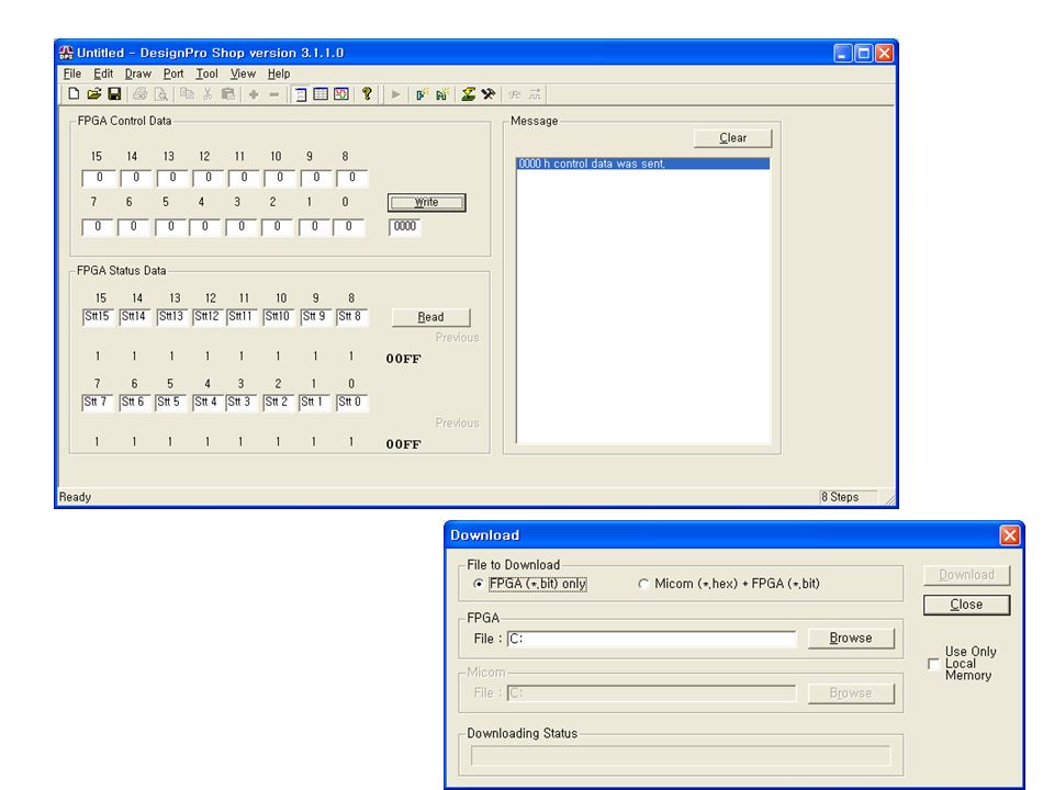
20
How to emulate with DPS –Double click DPS 3.1 –select Tool Download –push Browse and select myinv.bit –Successfully Downloaded message appears. –View Single Step Mode, input signals and click Write –View Waveform Mode, you can see the waves

22
View Multi Step Mode –Edit Add : lines appear(or click ‘+’ symbol). –Input 16 digits either in Binary or Hexa. ex) 0000000000001000 or 0008 (which is simpler?) –Edit Select All (or Ctrl-C). –Port Run (or symbol ’ ’):automatically processes and outputs generated in binary and hexa. Tool Option Timing –Interval For Running 500ms may be changed.
 or 0008 (which is simpler ) –Edit Select All (or Ctrl-C). –Port Run (or symbol ’ ’):automatically processes and outputs generated in binary and hexa. Tool Option Timing –Interval For Running 500ms may be changed..")
23
Multi Step Mode

24
Multi Step Mode I/O Hexa-decimal input and hexa-decimal output is recommended Without input, rest of the digits are filled with zero automatically. When not connected by cable, the hexa- decimal digit is F’s(1111) –ex1) 16 = (1111 0000), hence F0. –ex2) 9 = (1111 1001) hence F9.
 –ex1) 16 = ( ), hence F0. –ex2) 9 = ( ) hence F9..")
25
DPS Emulation Result 15 14 13 12 11 10 9 8 7 6 5 4 3 2 1 0 0 0 0 0 0 0 0 0 0 0 0 0 0 0 0 0 0 1 1 1 1 1 1 1 1 1 1 1 1 1 1 0 0 FFFC 0 0 0 0 0 0 0 0 0 0 0 0 0 0 0 1 1 1 1 1 1 1 1 1 1 1 1 1 1 1 1 0 1 FFFD 0 0 0 0 0 0 0 0 0 0 0 0 0 0 1 0 2 1 1 1 1 1 1 1 1 1 1 1 1 1 1 0 1 FFFD 0 0 0 0 0 0 0 0 0 0 0 0 0 0 1 1 3 1 1 1 1 1 1 1 1 1 1 1 1 1 1 1 0 FFFE 0 0 0 0 0 0 0 0 0 0 0 0 0 1 0 0 4 1 1 1 1 1 1 1 1 1 1 1 1 1 1 0 1 FFFD 0 0 0 0 0 0 0 0 0 0 0 0 0 1 0 1 5 1 1 1 1 1 1 1 1 1 1 1 1 1 1 1 0 FFFE 0 0 0 0 0 0 0 0 0 0 0 0 0 1 1 0 6 1 1 1 1 1 1 1 1 1 1 1 1 1 1 1 0 FFFE 0 0 0 0 0 0 0 0 0 0 0 0 0 1 1 1 7 1 1 1 1 1 1 1 1 1 1 1 1 1 1 1 1 FFFF

Similar presentations

 Set up basic environment Select Gates or Modules to Be simulated (Insert Program Code) Run Waveform.>")


