Download presentation
Presentation is loading. Please wait.

1
Rapid Prototyping with PLDs 4 th & 7 th October 2005

2
Contents 1.PLD versus ASIC 2.Definitions: a)Rapid prototyping b)PLD 3.PLD a)Types of PLDs b)How PLDs remember their configuration c)PLD Advantages d)PLD Suppliers e)PLD Programming Languages 4.From Verilog to PLD prototyping
Rapid prototyping b)PLD 3.PLD a)Types of PLDs b)How PLDs remember their configuration c)PLD Advantages d)PLD Suppliers e)PLD Programming Languages 4.From Verilog to PLD prototyping")
3
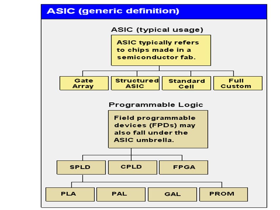
PLD versus ASICs ASICs – Application Specific ICs

5
DEFINITIONS Rapid Prototyping –“Pencontohsulongan cepat”. –Why do it? Saves cost. To test and verify functionality of a design, before the actual chip is fabricated. PLD –Programmable Logic Device.

6
PLD A programmable logic device. –Programmed by the customer. An electronic component used to build digital circuits. Has an undefined function at the time of manufacture. –Must be programmed before it can be used in a circuit. PROM and EPROM are also considered a PLD if they contain program codes (not just data).
..")
7
PLDs A single PLD is able to replace a circuit that consists of a few 7400-series TTL ICs. Function of the PLD is assigned during programming of the device, i.e. configuration. –This function may be changed during reprogramming (reconfiguration) of the PLD.
 of the PLD..")
8
Programmability of PLD 1.OTP, One-time Programmable PROM –Uses fuse links 2.Re-programmable Able to store logic design in: –EPROM – uv erasable –EEPROM- electrically erasable –SRAM –Flash memory

9
Types of PLDs 1.SPLD a)PAL (Programmable Array Logic) –The first PLD, introduced by Monolithic Memories, in 1970s. b)PLA (Programmable Logic Array) c)GAL (Generic Array Logic) –Invented by Lattice Semiconductor. 2.CPLD For bigger logic circuits, it can replace thousands, or even hundreds of thousands, of logic gates. 3.FPGA Based on gate-array technology. “Field” – an engineering term for the world outside the factory, i.e. where the customers are.
PLA (Programmable Logic Array) c)GAL (Generic Array Logic) –Invented by Lattice Semiconductor. 2.CPLD For bigger logic circuits, it can replace thousands, or even hundreds of thousands, of logic gates. 3.FPGA Based on gate-array technology. Field – an engineering term for the world outside the factory, i.e. where the customers are..")
10
Which PLD to choose? Based on: –Number of gates available, i.e. device capacity. –Speed. –Cost. –Volatility. –Power consumption. –Number of I/O pins. FPGAs and CPLDs are equally good choices for a particular task.

11
Which PLD to choose? CPLD: thousands to tens of thousands gates.

12
Switch Matrix Determines interconnection of logic block with the routing wires.

13
Max7128S Floorplan

14
Which PLD to choose? FPGA: tens of thousands to several million gates. Xilinx Virtex – 8 million gates.

15
Flex10k Floorplan

16
Interconnection Switch Box The programmable switches will determine whether or not a horizontal line is connected to the vertical line intersecting it. What makes this possible?

17
FPGA FPGA versus MPGA (Mask Programmable Gate Array). Configuration is volatile, and must be reloaded each time on power-up. –Use external PROM or EPROM to store configuration data. Configuration may be changed if a different functionality is required, via reconfiguration.

18
FPGA Contains programmable logic blocks, and may include programmable interconnects and switches

19
FPGA Applications ASIC Prototyping DSP Aerospace and defense systems Medical Imaging Computer Vision Speech Recognition Cryptography Bioinformatics

20
Other types of PLDs 1.Reconfigurable systems –Microprocessor circuits that contain some fixed functions and other functions that can be altered when the processor is running. –Self-altering systems. –The reconfigured FPGA can even test the host system that it is embedded, i.e. BIST, Built-in Self Test. –Includes “internet reconfigurable logic, IRL”.

21
Other types of PLDs 2.Flash –An EEPROM chip. –Can erase memory in "in a flash“. –Used for storage modules such as USB drives, digital camera, memory cards and fax machines. –Flash BIOS chips replaced ROM BIOS chips in PCs so that the BIOS could be updated in place (on board) instead of being removed and replaced.
 instead of being removed and replaced..")
22
FLASH MEMORY

23
How PLDs remember their configuration Anti-fuse –Normally open, until a programming current (~5mA) is forced through it. EPROM cells –MOS transistor that is switched on by trapping an electric charge permanently on its gate electrode. The charge remains for many years and can only be removed by exposing the chip to strong ultraviolet (uv) light. EEPROM cells –Also uses MOS transistor, but the charge trapped on the gate electrode is removed by applying a voltage of the opposite polarity. SRAM Flash memory
 light. EEPROM cells –Also uses MOS transistor, but the charge trapped on the gate electrode is removed by applying a voltage of the opposite polarity. SRAM Flash memory.")
24
PLD Advantages New chip designs can be tested and easily modified, without involving expensive photomask costs for chips completed in a semiconductor fab. Memory-based PLDs can be reprogrammed over and over, which allows for working products to be upgraded at the user’s site.

25
PLD Programming Languages Currently: –Verilog HDL –VHDL (Very High Speed IC HDL) –Altera HDL Used to be: –ABEL –CUPL –PALASM
 –Altera HDL Used to be: –ABEL –CUPL –PALASM")
26
PLD Suppliers Altera Xilinx Atmel Actel AT&T Lattice Cypress Quicklogic

27
From Verilog to PLD Prototyping

28
PLD Programming Functional simulation success? Synthesis – produces netlist, in EDIF (Electronic Design Interchange Format) format. Place & Route – mapping the actual structure described in the netlist onto actual macrocells, interconnections and IO pins of the PLD. This produces a bitstream, i.e. binary data to be loaded onto the FPGA or CPLD.
 format. Place & Route – mapping the actual structure described in the netlist onto actual macrocells, interconnections and IO pins of the PLD. This produces a bitstream, i.e. binary data to be loaded onto the FPGA or CPLD..")
29
PLD Programming 1.Uses “device programmer”. 2.Devices that are EEPROM or flash based technology are in-circuit programmable, i.e. the additional circuitry that is required to perform device (re) programming is provided inside the FPGA or CPLD itself. This is done with the aid of a JTAG interface or from on- board embedded processor.
 programming is provided inside the FPGA or CPLD itself. This is done with the aid of a JTAG interface or from on- board embedded processor..")
30
Downloading using the Byteblaster Cable

31
The Altera UP1 Download Board

32
Questions 1.Discuss the advantages of using FPGA as compared to standard ICs, like the TTL 7400 series and ASICs. 2.Name other forms of design entries besides HDL. 3.How is non-volatile data held for an FPGA device? 4.What are the advantages and disadvantages of the volatility characteristic of the FPGA? 5.Name applications of reconfigurable hardware.

33
6.For the Max7128S and Flex10k, a)How many gates does the device has? b)How many I/O pins? c)What is the speed of the device? d)Sketch and label its floorplan with the programmable elements inside it. Tip: Use data sheets which you can obtain from Altera’s website.
How many I/O pins. c)What is the speed of the device. d)Sketch and label its floorplan with the programmable elements inside it. Tip: Use data sheets which you can obtain from Altera’s website..")
34
What do you think?

Similar presentations

>")


 Boundary Scan Chen Shalom www.cs.huji.ac.il/~chensha.>")
 Terms of Use Chapter 3 – Combinational.>")

 Fixed OR array programmable AND array Fixed OR array programmable AND array Easy to program Easy to program Poor flexibility.>")


 Terms of Use Lecture 13 – Programmable.>")


