Download presentation
Presentation is loading. Please wait.

1
Chapter 6 – Digital Electronics – Part 1 1.D (Data) Flip Flops 2.RS (Set-Reset) Flip Flops 3.T Flip Flops 4.JK Flip Flops 5.JKMS Flip Flops Information Registers
 Flip Flops 2.RS (Set-Reset) Flip Flops 3.T Flip Flops 4.JK Flip Flops 5.JKMS Flip Flops Information Registers")
2
Flip-flop 1)may also refer to the bistable multivibrator, a circuit with two stable states (output). 2)Flip flips are used to store data (or information). 3)Different types of flip flops serve different functions. 4)Flip flops can be defined with characteristic functions.
Flip flips are used to store data (or information). 3)Different types of flip flops serve different functions. 4)Flip flops can be defined with characteristic functions..")
3
Flip flips store data on a rising or falling trigger edge. –Example: control input transitions from 0 1, data input appears at output –Data remains stable in the flip flop until next rising edge. Data Storage Lo-Hi Lo-Hi edge Hi-Lo Hi-Lo edge

4
A clock is a circuit that outputs 0’s and 1’s at specific frequencies A clock

5
LatchesFF Latches are Level Sensitive Out put is constantly affected by the input as long as enable is assertive. When enabled, their content changes immediately when input changes. sensitive to the duration of pulse and can transfer data until they are switched on. used as temporary buffers. One latch stores one bit of information Main types of latches are SR, D, JK, and T. Flip-Flops are Edge Sensitive. Content changes only either At the rising or falling edge of the enable signal. Enable signal is usually the controlling clock signal. sensitive to signal change (low to high or high to low) and not the level. used as registers. One FF stores one bit of information Main types of flip flops are SR, D, JK, and T. Latches and Flip Flops A clock
 and not the level. used as registers. One FF stores one bit of information Main types of flip flops are SR, D, JK, and T. Latches and Flip Flops A clock.")
6
The outputs of any single-bit latch or memory are traditionally designated Q and Q'. In a commercial latch circuit, either or both of these may be available for use by other circuits. In any case, the circuit itself is: 1) The Basic RS Latch NAND Latch
 The Basic RS Latch NAND Latch.")
8
NOR Latch

9
The Clocked RS NAND Latch

10
The Edge-Triggered RS Flip-Flop Symbols

11
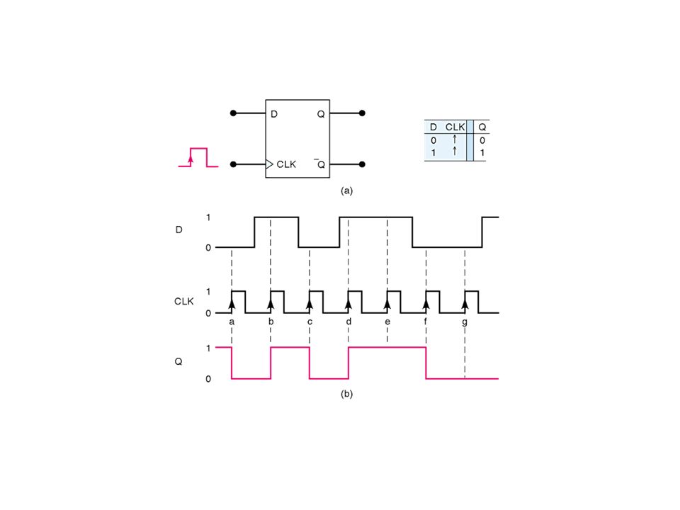
The D Latch & Flip Flop 0 1 1 1 1 0 X 0 Q 0 Q 0 D C Q Q When C is high, D passes from input to output (Q). Lo-Hi Lo-Hi edge Hi-Lo Hi-Lo edge

12
The D Flip-Flop

13
C DQ Q’ 0 0 1 1 1 0 X 0 Q 0 Q 0 ’ D C Q Q’ Positive edge triggered D Flip-Flop D gets latched to Q on the rising edge of the clock.

15
The JK Flip-Flop Symbols

16
Flip flops are powerful storage elements –They can be constructed from gates and latches! D flip flop is simplest and most widely used Asynchronous inputs allow for clearing and presetting the flip flop output Multiple flops allow for data storage –The basis of computer memory! Combine storage and logic to make a computation circuit Next time: Analyzing sequential circuits.

17
Random-Access Memory Can read and write at any point in memory Implemented using D Flip-Flops Register Used to hold one item of information CPU’s have many registers Clocks A clock is a circuit that outputs 0’s and 1’s at specific frequencies

18
Negative-Edge-Triggered T Flip-Flop

19
Latch and Flip-flop Timing

Similar presentations


 Shift Registers and Application Counters (Types,>")
 The slides included herein were taken from the materials accompanying Fundamentals.>")


 Department of Computer Science Faculty.>")


