Download presentation
Presentation is loading. Please wait.

6
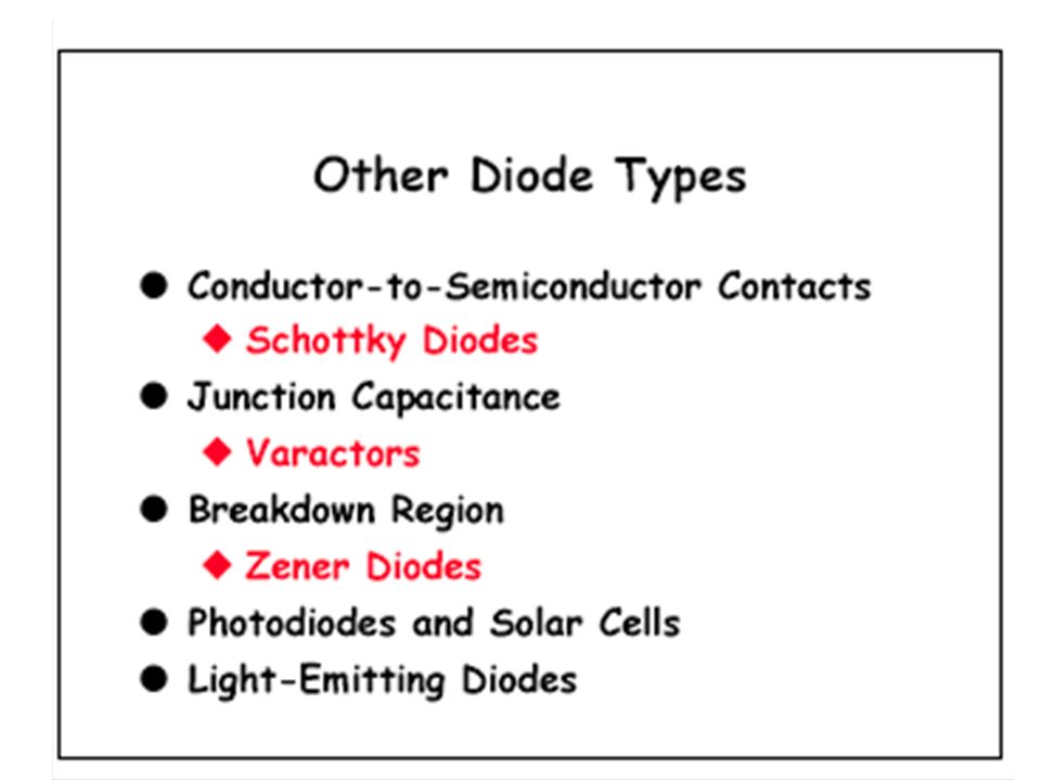
Schottky Barrier Diode
One semiconductor region of the pn junction diode can be replaced by a non-ohmic rectifying metal contact.A Schottky contact is easily formed on n-type silicon. The metal region becomes the anode. An n+ region is added to ensure that the cathode contact is ohmic. Schottky diodes turn on at a lower voltage than pn junction diodes and have significantly reduced internal charge storage under forward bias.

14
Circuit symbol for the variable capacitance diode (Varactor)
Diodes can be designed with hyper-abrupt doping profiles that optimize the reverse-biased diode as a voltage controlled capacitor. Circuit symbol for the variable capacitance diode (Varactor) Chap 3 -14
 Chap")
18
Reverse Bias External reverse bias adds to the built-in potential of the pn junction. The shaded regions below illustrate the increase in the characteristics of the space charge region due to an externally applied reverse bias, vD.

19
Reverse Bias (cont.) External reverse bias also increases the width of the depletion region since the larger electric field must be supported by additional charge.

20
Reverse Bias Saturation Current
We earlier assumed that the reverse saturation current was constant. Since it results from thermal generation of electron-hole pairs in the depletion region, it is dependent on the volume of the space charge region. It can be shown that the reverse saturation gradually increases with increased reverse bias. IS is approximately constant at IS0 under forward bias.

21
Reverse Breakdown 2 V < VZ < 2000 V
Increased reverse bias eventually results in the diode entering the breakdown region, resulting in a sharp increase in the diode current. The voltage at which this occurs is the breakdown voltage, VZ. 2 V < VZ < 2000 V

22
Reverse Breakdown Mechanisms
Avalanche Breakdown Si diodes with VZ greater than about 5.6 volts breakdown according to an avalanche mechanism. As the electric field increases, accelerated carriers begin to collide with fixed atoms. As the reverse bias increases, the energy of the accelerated carriers increases, eventually leading to ionization of the impacted ions. The new carriers also accelerate and ionize other atoms. This process feeds on itself and leads to avalanche breakdown.

23
Reverse Breakdown Mechanisms (cont.)
Zener Breakdown Zener breakdown occurs in heavily doped diodes. The heavy doping results in a very narrow depletion region at the diode junction. Reverse bias leads to carriers with sufficient energy to tunnel directly between conduction and valence bands moving across the junction. Once the tunneling threshold is reached, additional reverse bias leads to a rapidly increasing reverse current. Breakdown Voltage Temperature Coefficient Temperature coefficient is a quick way to distinguish breakdown mechanisms. Avalanche breakdown voltage increases with temperature, whereas Zener breakdown decreases with temperature. For silicon diodes, zero temperature coefficient is achieved at approximately 5.6 V. Chap 3 -23

24
Breakdown Region Diode Model
In breakdown, the diode is modeled with a voltage source, VZ, and a series resistance, RZ. RZ models the slope of the i-v characteristic. Diodes designed to operate in reverse breakdown are called Zener diodes and use the indicated symbol. Chap 3 -24

27
Photo Diodes and Photodetectors
If the depletion region of a pn junction diode is illuminated with light with sufficiently high frequency, photons can provide enough energy to cause electrons to jump the semiconductor bandgap to generate electron-hole pairs: h =Planck’s constant = x J-s = frequency of optical illumination l = wavelength of optical illumination c = velocity of light = 3 x 10⁸ m/s Photon-generated current can be used in photodetector circuits to generate an output voltage The diode is reverse-biased to enhance depletion-region width and electric field.

37
Rectifier Circuits A basic rectifier converts an ac voltage to a pulsating dc voltage. A filter then eliminates ac components of the waveform to produce a nearly constant dc voltage output. Rectifier circuits are used in virtually all electronic devices to convert the 120-V 60-Hz ac power line source to the dc voltages required for operation of electronic devices. In rectifier circuits, the diode state changes with time and a given piecewise linear model is valid only for a certain time interval. Chap 3 -37

38
Half Wave Rectification

40
Figure 2.6 Full-wave rectifier: (a) circuit with center-tapped transformer, (b) voltage transfer characteristics, and (c) input and output waveforms
 circuit with center-tapped transformer, (b) voltage transfer characteristics, and (c) input and output waveforms.")
41
Full-Wave Rectifiers Full-wave rectifiers cut capacitor discharge time in half and require half the filter capacitance to achieve a given ripple voltage. All specifications are the same as for half-wave rectifiers. Reversing polarity of the diodes gives a full-wave rectifier with negative output voltage.

42
Figure 2.7 A full-wave bridge rectifier: (a) circuit showing the current direction for a positive input cycle, (b) current direction for a negative input cycle, and (c) input and output voltage waveforms
 circuit showing the current direction for a positive input cycle, (b) current direction for a negative input cycle, and (c) input and output voltage waveforms.")
43
Full-Wave Bridge Rectification
The requirement for a center-tapped transformer in the full-wave rectifier is eliminated through use of 2 extra diodes. All other specifications are the same as for a half-wave rectifier except PIV = VP. Chap 3 -43

45
Rectifier Topology Comparison
Filter capacitors are a major factor in determining cost, size and weight in design of rectifiers. For a given ripple voltage, a full-wave rectifier requires half the filter capacitance as that in a half-wave rectifier. Reduced peak current can reduce heat dissipation in diodes. Benefits of full-wave rectification outweigh increased expenses and circuit complexity (an extra diode and center-tapped transformer). The bridge rectifier eliminates the center-tapped transformer, and the PIV rating of the diodes is reduced. Cost of extra diodes is negligible. Chap 3 -45
. The bridge rectifier eliminates the center-tapped transformer, and the PIV rating of the diodes is reduced. Cost of extra diodes is negligible. Chap")
48
Half-wave rectifier with filter

Similar presentations


, Aluminum (Al), Gallium (Ga), Indium (ln). Has three (3) valence.>")


