Download presentation
Presentation is loading. Please wait.

1
ECE 875: Electronic Devices Prof. Virginia Ayres Electrical & Computer Engineering Michigan State University ayresv@msu.edu

2
VM Ayres, ECE875, S14 Chp 03: metal-semiconductor junction: INTERCONNECTS Practical detail: Work functions graph Lecture 26, 17 Mar 14 Chp 04: metal-insulator-semiconductor junction: GATES Basics Examples

3
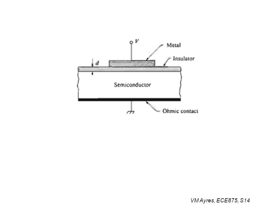
VM Ayres, ECE875, S14

4
Chp 03: metal-semiconductor junction: INTERCONNECTS Practical details: Work functions graph Useful experiments Lecture 26, 17 Mar 14 Chp 04: metal-insulator-semiconductor junction: GATES Basics Examples

5
Chp. 01: Si Chp. 02: pn Chp. 03: Interconnect Chp. 04: MOS: Gate VM Ayres, ECE875, S14

7
++++++++++ oooooooooo p-type Si + charge on gate: Holes moved out under gate VM Ayres, ECE875, S14

8
++++++++++ oooooooooo p-type Si: N A =B B- B- B- B- B- + charge on gate Holes moved out under gate B- depletion region left behind VM Ayres, ECE875, S14

9
++++++++++ oooooooooo p-type Si: N A =B B- B- B- B- B- Increase the + charge on gate Holes moved out under gate B- depletion region left behind Electrons attracted under gate ++++++++++ e- e- e- e- e- VM Ayres, ECE875, S14

10
oooooooooo p-type Si: N A =B B- B- B- B- B- Change: Big - charge on gate Extra holes attracted under gate B- depletion region left behind - - - - - Super p+ Normal p-type VM Ayres, ECE875, S14

11
p-type Si VM Ayres, ECE875, S14

12
p-type “Ideal”: Miraculous choice of metal and semiconductor that achieves flat band: E Fm = E Fs for V= 0 At equilibrium: V = 0 volts, ideal case: VM Ayres, ECE875, S14

13
p-type - V rev + V rev breaks invariance of E F Brings it down by amount V rev E i – E F greater near surface More holes near surface Accumulation of holes near surface Hole layer near surface Super p+Normal p-type Also have B- layer VM Ayres, ECE875, S14 In V rev : starting from ideal case:

14
p-type + V for - E i – E F smaller near surface Less holes near surface Can become intrinsic near surface V for breaks invariance of E F Brings it up by amount V for In V for : starting from ideal case: VM Ayres, ECE875, S14

15
p-type + V for - V for breaks invariance of E F Brings it up by amount V for Now have E F – E i > 0 Electron layer in p-type Si near surface: Inversion Also have B- depletion region near surface In V for : VM Ayres, ECE875, S14

16
Charge layers near surface: inversion This is similar to Pr. 2.04 Pr. 2.04 turns up in many different circumstances New: ++ charges on gate In V for : VM Ayres, ECE875, S14

17
New: Battery voltage V is accommodated as drops V i across the insulator and s = the surface potential (ideal flat band conditions) Charge layers near surface: inversion In V for : starting from ideal case: E –field and potential VM Ayres, ECE875, S14
 Charge layers near surface: inversion In V for : starting from ideal case: E –field and potential VM Ayres, ECE875, S14")
18
Metal = battery potential: V p-type Semiconductor potential: p (x) New: the potential drop across the (ideal) insulator V i Semiconductor surface potential: s = p (x=0) Electric field and potentials near surface: in inversion: VM Ayres, ECE875, S14
 New: the potential drop across the (ideal) insulator V i Semiconductor surface potential: s = p (x=0) Electric field and potentials near surface: in inversion: VM Ayres, ECE875, S14")
19
Grad E ∞ means deep in substrate The total charge density is The Electric field is a function of the charge density. The potential is proportional to the Electric field The surface charge is: In semiconductor: VM Ayres, ECE875, S14

20
(x) VM Ayres, ECE875, S14
 VM Ayres, ECE875, S14")
21
Chp 03: metal-semiconductor junction: INTERCONNECTS Practical details: Work functions graph Useful experiments Lecture 26, 17 Mar 14 Chp 04: metal-insulator-semiconductor junction: GATES Basics Examples

22
Example 01 (will be a continuing problem): + VM Ayres, ECE875, S14
: + VM Ayres, ECE875, S14")
23
Answer: VM Ayres, ECE875, S14

24
Name these: p p0 = p p (x = ∞) and n p0 = n p (x = ∞) Want: p p (x) and n p (x) as they get near to the junction Can evaluate something related to p p (∞) and n p0 = n p (∞) first VM Ayres, ECE875, S14
 and n p0 = n p (x = ∞) Want: p p (x) and n p (x) as they get near to the junction Can evaluate something related to p p (∞) and n p0 = n p (∞) first VM Ayres, ECE875, S14")
25
Instead of just filling in for N A- and N D+, consider this: VM Ayres, ECE875, S14 Something is: (N D + - N A -): Example 01: You just got numbers for these Next
: Example 01: You just got numbers for these Next")
26
Instead of just filling in for N A- and N D+, consider this: Use p set-up as a clue VM Ayres, ECE875, S14 Something is: (N D + - N A -): Example 01: You just got numbers for these
: Example 01: You just got numbers for these")
27
Can find: p p (x) and n p (x) from energy band considerations: VM Ayres, ECE875, S14
 and n p (x) from energy band considerations: VM Ayres, ECE875, S14")
28
Can find: p p (x) and n p (x) from energy band considerations: Note: voltage p = p (x) VM Ayres, ECE875, S14
 and n p (x) from energy band considerations: Note: voltage p = p (x) VM Ayres, ECE875, S14")
29
Therefore have: = p (x) VM Ayres, ECE875, S14
 VM Ayres, ECE875, S14")
30
Example: VM Ayres, ECE875, S14

31
Answer: VM Ayres, ECE875, S14

32
Also: Can find surface potential s (x=0) using condition: 2 x Bp = VM Ayres, ECE875, S14
 using condition: 2 x Bp = VM Ayres, ECE875, S14")
33
Example: Evaluate s in strong inversion condition for example problem 01 with N A = 4 x 10 15 cm -3 VM Ayres, ECE875, S14

34
Answer: VM Ayres, ECE875, S14 Note: voltage s = p (x = 0)
")
Similar presentations


 junctions>")


