Download presentation
Presentation is loading. Please wait.

1
ECSE-6290 Semiconductor Devices and Models II Lecture 20: Laser Diodes
Shayla M. Sawyer Bldg. CII, Room 8225 Rensselaer Polytechnic Institute Troy, NY Tel. (518) FAX (518)
 FAX (518)")
2
Lecture Outline Introduction Main Concepts Laser Diode Types
Stimulated Emission Population Inversion Optical Gain Optical Resonator Threshold Current Laser Diode Types

3
Concepts: Population Inversion
Switch from two energy levels to two separate continuous bands Electron concentration as a function of energy, determined by Fermi-Dirac distribution and Density of States Population Inversion T>0K Population Inversion T=0K Equilibrium

4
Concepts: Population Inversion and Optical Gain
Photons above EFn-EFp are absorbed

5
Concepts: Population Inversion and Optical Gain

6
Laser Physics: Population Inversion
Necessary requirements and conditions for lasing In order for equation below to be positive FC>FV and EFn>EFp (population inversion) Photon energy must be larger than the bandgap For current pumped laser diode the quantity (EFn-EFp) is equal to the bias voltage, bias is limited to the built up potential of the junction (ψBn+ ψBp) Fermi-Dirac For homojunction: one side must be doped to degeneracy
 Photon energy must be larger than the bandgap. For current pumped laser diode the quantity (EFn-EFp) is equal to the bias voltage, bias is limited to the built up potential of the junction (ψBn+ ψBp) Fermi-Dirac. For homojunction: one side must be doped to degeneracy.")
7
Concepts: Optical Resonator
Need to build up stimulated emissions by a optical resonator Provided by cleaved and polished ends of the crystal

8
Concepts: Optical Resonator
Requirement is a structure to trap the light and build up intensity inside Like a Fabry-Perot etalon, two parallel walls perpendicular to the junction Longitudinal modes: multiple resonant frequencies Separation of modes in wavelength and frequency Only multiples of the half wavelength can exist in the cavity Output spectrum is determined by the optical cavity, and optical gain vs. wavelength characteristics

9
Concepts: Optical Gain
Optical gain (g) due to stimulated emission is compensated by optical loss due to absorption (α) Net gain/loss as a function of distance For a given system R1, R2, and α are fixed, the only parameter to vary is overall gain To keep gain positive Threshold gain
 due to stimulated emission is compensated by optical loss due to absorption (α) Net gain/loss as a function of distance. For a given system R1, R2, and α are fixed, the only parameter to vary is overall gain. To keep gain positive. Threshold gain.")
10
Concepts: Threshold Current
The relationship between optical gain and bias current can be described by the equation Linear increase of optical gain with bias current Nominal current density Threshold value

11
Concepts: Threshold Current
Lasing oscillations occur only when the optical gain in the medium can overcome the photon losses from the cavity Cavity modes vary with increasing current

12
double heterostructure
Laser Types single heterostructure double heterostructure homostructure

13
Both Carrier and Optical Confinement!

14
Example: Modes in an optical cavity length
Consider an AlGaAs based heterostructure laser diode which has an optical cavity of length 200 microns. The peak radiation is at 870 nm and the refractive index of GaAs is about 3.7. a) What is the mode integer m of the peak radiation and the separation between modes of the cavity? b) If the optical gain vs. wavelength characteristics has a FWHM wavelength width of about 6 nm, how many modes are there within this bandwidth? c) How many modes are there if the cavity length is 20 μm?
 What is the mode integer m of the peak radiation and the separation between modes of the cavity b) If the optical gain vs. wavelength characteristics has a FWHM wavelength width of about 6 nm, how many modes are there within this bandwidth c) How many modes are there if the cavity length is 20 μm")
15
Gain guided: optical gain is highest where current density is greatest
Stripe contact increases current density in the active region. The widths of the active region or the optical gain region is defined by current density from the stripe Gain guided: optical gain is highest where current density is greatest

16
Index guided: optical power confined to waveguide
Active layer is surrounded by lower index AlGaAs and behaves like a dielectric waveguide Ensures that photons are confined to the active or optical gain region Increases rate of stimulated emission Index guided: optical power confined to waveguide

17
Index guided LD: changes from multiple mode to single mode with increasing optical power
Gain guided: remain multimode even at high diode currents

18
Single Frequency Solid State Lasers: DBR laser
Frequency selective dielectric mirrors a cleaved surfaces. Only allow a single mode to exist Periodic corrugated structure that interfere constructively when the wavelength corresponds to twice the corrugation periodicity (Bragg wavelengths)
")
19
Single Frequency Solid State Lasers: DFB laser
The corrugated layer, called the guiding layer, is now next to the active layer In the DFB structure traveling wave are reflected partially and periodically as they propogate.

20
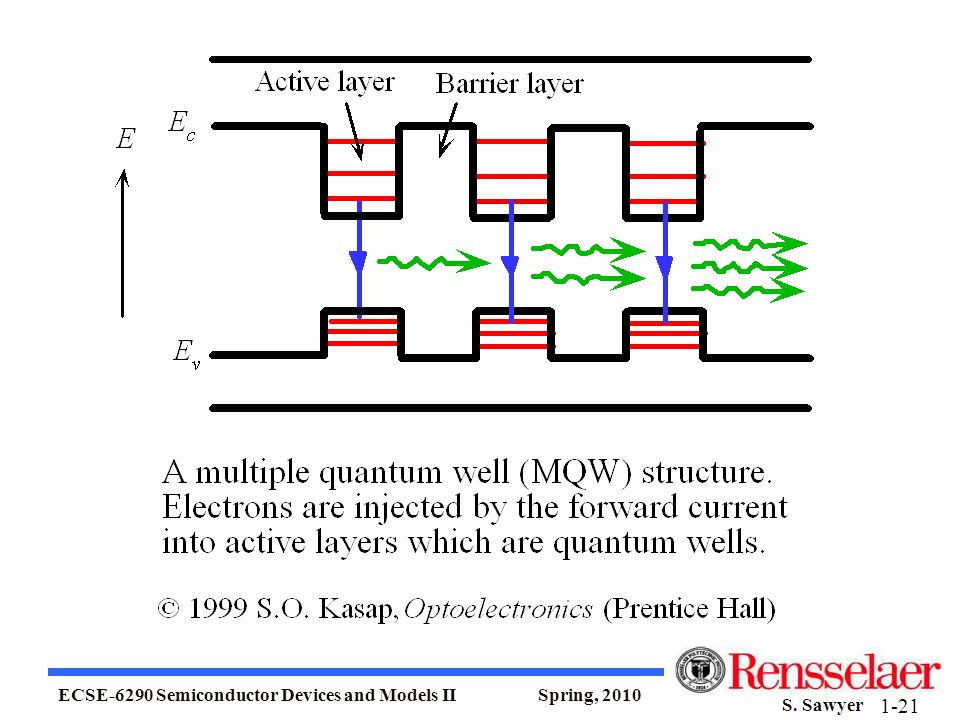
Constant 2D density of states means a large concentration of electron can easily occur at E1 (and holes at the minimum valence band energy) Population inversion occurs quickly without the need for a large current to bring a large number of electrons Benefits: Threshold current reduced, linewidth is narrower

22
Optical cavity axis along the direction of current flow rather than perpendicular to current flow
Radiation emerges from the surface of the cavity rather than from its edge Reflectors at the edges of the cavity are dielectric mirrors 20-30 layers for mirror, MQW active region

23
Summary Laser concepts: Stimulated Emission, Population Inversion, Optical Resonator, Optical Gain, and Laser Threshold Current Types of laser diodes include Homostructure Single heterostructure Double heterostructure Gain guided (stripe geometry) Index guided (buried heterostructure) Distributed Bragg reflection Distributed feedback Quantum well, multiple quantum well Vertical cavity surface emitting
 Index guided (buried heterostructure) Distributed Bragg reflection. Distributed feedback. Quantum well, multiple quantum well. Vertical cavity surface emitting.")
24
ECSE-6290 Semiconductor Devices and Models II Lecture 21: Photodetectors
Prof. Shayla M. Sawyer Bldg. CII, Room 8225 Rensselaer Polytechnic Institute Troy, NY Tel. (518) FAX (518)
 FAX (518)")
25
Lecture Outline Introduction to Photodetectors Photodiodes
General p-i-n and p-n Metal-Semiconductor Avalanche Metal-Semiconductor-Metal Photodetector Quantum Well Infrared Photodetector Summary

26
Introduction Photodetectors are semiconductor devices that can detect optical signals through electronic processes Three main processes: Carrier generation by incident light Carrier transport and/or multiplication by current-gain mechanism Extraction of carriers as terminal current to provide the output signal Desired: High sensitivity, high response speed, minimum noise, compact size, low biasing voltage and current

27
Introduction Wavelength relation to transition energy
ΔE is the transition of energy levels Depending on photodetector type can be: Energy gap of the semiconductor Barrier height as in a metal semiconductor photodiode Transition energy between impurity level and band edge as an extrinsic photoconductor Often minimum wavelength for detection

28
Introduction Important Factors/Parameters Absorption Coefficient
Response Speed Quantum Efficiency Responsivity Gain Noise Detectivity

29
Introduction Absorption coefficient
Determines whether light can be absorbed for photoexcitation Determines where light is absorbed High value means near surface Low value means deeper penetration

30
Introduction Response Speed Quantum Efficiency
Shorter carrier lifetime yields fast response at the expense of higher dark current (noise) Depletion width should be shortened to reduce transit time at the expense of capacitance Quantum Efficiency Number of carriers produced per photon Iph is the photocurrent, Φ is the photon flux (=Popt/hv) and Popt is the optical power
 Depletion width should be shortened to reduce transit time at the expense of capacitance. Quantum Efficiency. Number of carriers produced per photon. Iph is the photocurrent, Φ is the photon flux (=Popt/hv) and Popt is the optical power.")
31
Introduction Responsivity: Photocurrent generated per incident optical power Gain and response time for common photodetectors

32
Introduction Noise ultimately determines minimum detectable signal strength Sources of noise Dark current Thermal noise Shot noise Flicker noise Generation recombination noise Figure of Merit Noise Equivalent Power Detectivity A is the Area B is the Bandwidth NEP-incident rms optical power required to produce a signal-to-noise ratio of one in a 1 Hz bandwidth (minimum detectable light power)
")
33
Introduction Detectivity
The signal-to-noise ratio when one watt of light power is incident on a detector of area 1 cm2 measured over 1 Hz bandwidth Normalized to area, noise is generally proportional to the square root of area Detectivity depends on Detector sensitivity Spectral Response Noise Is a function of wavelength, modulation frequency and bandwidth

34
Photodiodes: General Photodiodes have depleted region with a high electric field that separates photogenerated electron-hole pairs Tradeoff between speed of response and quantum efficiency (depletion layer: transit time, absorbance area) Reverse biasing often employed to reduce carrier transit time and lower diode capacitance All photodiodes except Avalanche has a maximum gain of one a) p-i-n photodiodes b) pn photodiode c) Metal-i-n photodiode d) Metal-semiconductor photodiode e) Point contact photodiode
 Reverse biasing often employed to reduce carrier transit time and lower diode capacitance. All photodiodes except Avalanche has a maximum gain of one. a) p-i-n photodiodes b) pn photodiode c) Metal-i-n photodiode d) Metal-semiconductor photodiode e) Point contact photodiode.")
35
Photodiodes: General Important characteristics Quantum efficiency
Absorption coefficient strong dependence on wavelength Long wavelength cutoff given by energy gap of semiconductor Short wavelength cutoff given by large value of α (surface where recombination is likely) Response Speed Limited by Drift time in the depletion region Diffusion of carriers Capacitance of detection region Optimized when the depletion layer is chosen so the transit time is on the order of one half the modulation period WD ~ 1/α
 Response Speed. Limited by. Drift time in the depletion region. Diffusion of carriers. Capacitance of detection region. Optimized when the depletion layer is chosen so the transit time is on the order of one half the modulation period. WD ~ 1/α.")
36
Photodiodes: General Device Noise Shot noise Thermal noise where
IP average photocurrent, IB background radiation, ID dark current due to thermal generation of electron hole pairs in the depletion region Thermal noise where Rj Junction resistance Ri Input resistance of amplifier RL External load resistor

37
Photodiodes: General Signal to Noise for 100% modulated signal with average power Popt Minimum optical power required to obtain a given signal-to-noise ratio is (setting Ip=0) Noise equivalent power (S/N=1; B=1 Hz)
 Noise equivalent power (S/N=1; B=1 Hz)")
38
Photodiodes: p-i-n and p-n
Depletion layer thickness (intrinsic layer) can be tailored to optimize the quantum efficiency and frequency response Total photocurrent density through reverse biased depletion layer Total current density is the sum of Idr inside the depletion region and Idiff outside the depletion region
 can be tailored to optimize the quantum efficiency and frequency response. Total photocurrent density through reverse biased depletion layer. Total current density is the sum of Idr inside the depletion region and Idiff outside the depletion region.")
39
Photodiodes: p-i-n and p-n
Drift current equation For x>WD the minority carrier density (holes) is the bulk semiconductor is determined by the 1D diffusion equation Solution under boundary conditions pn=pno for x=∞, and pn=0 for x=WD
 is the bulk semiconductor is determined by the 1D diffusion equation. Solution under boundary conditions pn=pno for x=∞, and pn=0 for x=WD.")
40
Photodiodes: p-i-n and p-n
Diffusion current density is given by Total current density is the sum of Idr inside the depletion region and Idiff outside the depletion region

41
Photodiodes: p-i-n and p-n
Quantum efficiency Reduced from unity from Reflection R Light absorbed outside the depletion region High quantum efficiency, low R and αWD>>1 is desirable For WD>>1/ α transit time delay may be considerable

42
Photodiodes: p-i-n and p-n
Frequency Response Phase difference between photon flux and photocurrent will appear when incident light intensity is modulated rapidly Assume light is absorbed at surface, applied voltage is high enough to ensure saturation velocity Response time is limited by the carrier transit time through the depletion layer Compromise for high frequency response and quantum efficiency Absorption region of thickness 1/α to 2/α Large portion of light is absorbed within the depletion region

43
Photodiodes: p-i-n and p-n
Frequency Response 3-dB frequency Illustrates trade off between response speed and quantum efficiency at various wavelengths by adjusting the depletion width Smaller WD, shorter transit time, higher speed, but reduced η Shows internal quantum efficiency of the Si p-i-n photodiode as a function of the 3-dB frequency and depletion width

44
Examples: Speed and Responsivity
Operation and speed of a p-i-n photodiode A Si pin photodiode has an i-Si layer of width 20 μm. The p+ layer on the illumination side is very thin (0.1 μm). The pin is reverse biased by a voltage of 100 V and then illuminated with a very short optical pulse of wavelength 900 nm. What is the duration of the photocurrent if absorption occurs over the whole i-Si layer? 44
. The pin is reverse biased by a voltage of 100 V and then illuminated with a very short optical pulse of wavelength 900 nm. What is the duration of the photocurrent if absorption occurs over the whole i-Si layer 44.")
45
Examples: Speed and Responsivity
The absorption coefficient at 900 nm ~ 3 x 10⁴ m-1 so that the absorption depth is ~33 μm (from Figure). Assume that the absorption and hence photogeneration occurs over the entire width W of the i-Si layer. The field in the i-Si layer is At this field the electron drift velocity ve is very near its saturation at 105 m/s, whereas the hole drift velocity vh, is about 7x10⁴ m/s. Holes are slightly slower than the electrons. The transit time th of holes across the i-Si layer is To improve response time, the width of the i-Si layer has to be narrowed but it decreases the quantity of absorbed photons and reduces responsivity. 45
. Assume that the absorption and hence photogeneration occurs over the entire width W of the i-Si layer. The field in the i-Si layer is. At this field the electron drift velocity ve is very near its saturation at 105 m/s, whereas the hole drift velocity vh, is about 7x10⁴ m/s. Holes are slightly slower than the electrons. The transit time th of holes across the i-Si layer is. To improve response time, the width of the i-Si layer has to be narrowed but it decreases the quantity of absorbed photons and reduces responsivity. 45.")
46
Examples: Speed and Responsivity
Responsivity of a p-i-n photodiode A Si pin photodiode has an active light receiving area of diameter 0.4mm. When radiation of wavelength 700 nm (red light) and intensity 0.1 mW cm-2 is incident it generates a photocurrent of 56.6 nA. What is the responsivity and QE of the photodiodes at 700 nm? The incident light intensity 0.1 mW cm-2 means that the incident power for conversion is The responsivity is QE can be found from 46
 and intensity 0.1 mW cm-2 is incident it generates a photocurrent of 56.6 nA. What is the responsivity and QE of the photodiodes at 700 nm The incident light intensity 0.1 mW cm-2 means that the incident power for conversion is. The responsivity is QE can be found from. 46.")
47
Photodiodes: p-i-n and p-n
p-n photodiode Thin depletion layer means some light can be absorbed outside Light more than a diffusion length outside do not contribute at all to photocurrent Reduces quantum efficiency Diffusion process is slow Time require to diffuse a distance x Lower response speed than p-i-n Neutral region contributes to noise

48
Photodiodes: Heterojunction
Advantages Large bandgap material can be transparent and used as a window for transmission of incoming optical power Quantum efficiency is not dependent on distance of junction from surface Unique material combinations so quantum efficiency and response speed can be optimized for a given optical wavelength Reduced dark current J.H. Jang et al., Journal of Lightwave Technology, Vol. 20, No. 3, March 2002.

49
Photodiodes: Metal-Semiconductor
Has a threshold of qΦB, when it gets to the energy gap value the quantum efficiency jumps to a much high value Operates in two modes hυ>Eg : radiation produces electron hole pairs (similar to pin photodiode) hυ<Eg : photoexcited electrons surmount barrier
 hυ<Eg : photoexcited electrons surmount barrier.")
50
Photodiodes: Metal-Semiconductor
Quantum Efficiency in two modes hυ>Eg : radiation produces electron hole pairs (similar to p-i-n) hυ<Eg : photoexcited electrons surmount barrier, internal photoemission Internal photoemission has typical quantum efficiencies of less than 1% CF is the Fowler emission coefficient
 hυ<Eg : photoexcited electrons surmount barrier, internal photoemission. Internal photoemission has typical quantum efficiencies of less than 1% CF is the Fowler emission coefficient.")
51
Photodiodes: Metal-Semiconductor
Configurations Advantageous for band-to-band Diode illuminated through thin metal contact with antireflection coating Use low doping i layer similar to p-i-n Point contact diode reduces active volume, drift time and capacitance are small Very high modulation frequencies

52
Photodiodes: Metal-Semiconductor
Main advantages High speed and long wavelength detection capability without having to use a semiconductor with a small energy gap Not limited by charge storage of minority diffusion current Ultrafast Schottky barrier photodiodes beyond 100 GHz have been reported Useful in the visible and UV

53
Photodiodes: Avalanche
Operate at high reverse bias voltages where avalanche multiplication takes place Creates internal current gain Can respond to light modulated at microwave frequencies Current gain-bandwidth product of an APD can be higher than 300 GHz High gain comes at the price of noise Low frequency avalanche gain αn and αp are electron and hole ionization rates

54
Photodiodes: Avalanche
For equal ionization coefficients (α =αn=αp) multiplication takes the simple form In a practical device, the dc multiplication at high light intensities is limited by series resistance and space-charge effect Breakdown when αWD=1 I total multiplied current IP unmultiplied current ID unmultiplied dark current IMD multiplied dark current VR Reverse bias voltage VB Breakdown voltage
 multiplication takes the simple form. In a practical device, the dc multiplication at high light intensities is limited by series resistance and space-charge effect. Breakdown when αWD=1. I total multiplied current. IP unmultiplied current. ID unmultiplied dark current. IMD multiplied dark current. VR Reverse bias voltage. VB Breakdown voltage.")
55
Photodiodes: Avalanche
For high light intensity (IP >> ID) and IRs << VB, the maximum value of the photomultiplication is given by Avalanche multiplication noise Lower noise factor for electron injection because αn is much larger than αp in Si max Noise factor: Measure of shot noise increase compared to ideal noiseless multiplier
 and IRs << VB, the maximum value of the photomultiplication is given by. Avalanche multiplication noise. Lower noise factor for electron injection because αn is much larger than αp in Si. max. Noise factor: Measure of shot noise increase compared to ideal noiseless multiplier.")
56
Photodiodes: Avalanche
To achieve low noise and wide bandwidth in an APD Ionization coefficients of the carriers should be as different as possible Avalanche process should be initiated by the carrier species with a higher ionization rate Other species with lower ionization rate should be kept to a minimum as primary photogenerated current

57
Photodiodes: Avalanche
Current gain mechanism multiples the signal current, background current and dark current indiscriminately Signal to noise power ratio

58
Photodiodes: Avalanche
The previous equation can be solved for the minimum optical power Popt required to produce a given S/N with avalanche gain NEP can be improved by the reduction of Ieq by the gain M

59
Photodiodes: Avalanche
At high light power p-i-n detectors have larger SNR than APD There is a significant advantage of APDs for low light signals due to multiplication factor Optimization required for any system depending on optical flux SNR comparison between 1 mm2 diode detectors with a bandwidth 50Hz

60
Photodiodes: Avalanche
Material comparison Heterojunction avalanche photodiodes of III-V alloys advantages Wavelength response can be tuned High absorption coefficients of direct bandgap III-V alloys makes quantum efficiency high even if a narrow depletion width is used to provide a high speed response Heterostructure window layer can be grown Surface recombination loss minimized High speed performance

61
Photodiodes: Avalanche
Material comparison AlGaAs/GaAs, AlGaSb/GaSb, InGaAs/InP, and InGaAsP/InP Shown improvements in speed and quantum efficiency over Si and Ge Separation absorption and multiplication Higher bandgap material in the multiplication region Low bandgap material for light absorption Breakdown voltage is expected to vary as Eg2/3 so dark current due to tunneling is suppressed

62
Metal-Semiconductor-Metal Photodetectors
Basically two Schottky barriers connected back-to-back on a coplanar surface Added a thin barrier enhancement layer to reduce dark current Metal contacts have shape of interdigitated stripes Light is received at the gap between metal contacts For more complete light absorption, active layer has a thickness slightly larger than absorption length

63
Metal-Semiconductor-Metal Photodetectors
Typical operation Photocurrent first rises with voltage then becomes saturated Increase of photocurrent at low bias is due to expansion of the depletion region in the reverse biased Schottky junction and internal quantum efficiency improves Voltage at which photocurrent saturates corresponds to flat band condition Electric field at anode becomes zero Estimated by 1D depletion equation

64
Metal-Semiconductor-Metal Photodetectors
Main Drawback High dark current due to Schottky barrier junction Barrier enhancement layer can be added to reduce dark current of narrow energy gap semiconductor such as InGaAs Layer thickness ranges from 30 to 100nm Can be graded in composition to avoid carrier trapping

65
Metal-Semiconductor-Metal Photodetectors
Primary advantages High speed and compatibility with FET technology Planar structure easy to integrate on single chip Very low capacitance per area Advantageous for detectors requiring large light sensitive areas Compared to p-i-n capacitance is about half

66
Quantum Well Infrared Photodetectors
Structure of QWIP using GaAs/AlGaAs heterostructure QW layers 5nm doped to n-type in 1017 range Barrier layers are undoped and have a thickness 30-50nm Periods 20 to 50

67
Quantum Well Infrared Photodetectors
Incident light normal to surface has zero absorption Intersubband transition require electric field have components normal to QW plane Two methods Polished facet Grating to refract light Figure 716

68
Quantum Well Infrared Photodetectors
Intersubband excitation Three types of transitions Bound to bound (escape well by tunneling) Bound to continuum (escape well because first state is above barrier: easier) Bound to miniband in superlattice
 Bound to continuum (escape well because first state is above barrier: easier) Bound to miniband in superlattice.")
69
Quantum Well Infrared Photodetectors
I-V of QWIP is similar to photodetectors Quantum efficiency is different since light absorption and carrier generation occur only in quantum wells Nop number of optical passes, Nw number of quantum wells, Lw is the length, P is the polarization correction factor Ep is the escape probability and is a function of bias Ga is optical gain Cp is the capture probability of electron traversing quantum well tp transit time across single period of structure tt transit time across entire QWIP active length L

70
Quantum Well Infrared Photodetectors
Dark current is due to thermionic emission over the quantum well barriers and thermionic field emission (thermally assisted tunneling) near the barrier peaks To limit dark current, the QWIP has to be operated at low temperatures in the range of 4-77 K Can be applied in focal plane arrays for 2D imaging High speed capability and fast response Coupling of light to the photodetector is difficult
 near the barrier peaks. To limit dark current, the QWIP has to be operated at low temperatures in the range of 4-77 K. Can be applied in focal plane arrays for 2D imaging. High speed capability and fast response. Coupling of light to the photodetector is difficult.")
71
Summary Photodiodes have depleted region with a high electric field that separates photogenerated electron-hole pairs Width of depletion layer determines tradeoff between speed and quantum efficiency P-n photodiodes have lower response speed and higher noise than a p-i-n photodiode Heterojunction photodiodes can move light absorption region away from the surface due to transparence of larger bandgap materials MS photodiodes operate in two modes, used because no minority carriers that increases speed Avalanche photodiodes have high gain but at the cost of noise, better for signals of low light intensity MSM photodectors have high speed and large area but have high dark noise QWIP uses quantum wells and various intersubband transitions for electrons, and are often operated at low temperatures

Similar presentations


 radio to X-rays and beyond. Curtis Johnson Process.>")


>")


