Download presentation
Presentation is loading. Please wait.

1
Advanced Process Integration
ECE 7366 Advanced Process Integration Beyond Planar CMOS Dr. Wanda Wosik Text Book: B. El-Karek, “Silicon Devices and Process Integration”

2
Scaling of Bulk Planar Devices
2D retrograde well for Vt control L dependence long channel Vds short channel source/channel barrier Vds dependence Vgs log(Ids) Vds Vdd Ion Ioff long channel short channel Vds=0 Vds=Vdd Ioff is determined only by Vt and subthreshold swing SS (~Ctotal/Cox). The electrostatic control of the drain current by the gate gets lost Use additional (double) gate to recover the gate control over Ids Eliminate the path of the bulk leakage current – use oxide under the channel => SOI Reduce DIBL Improve Ion/Ioff
 Vds. Vdd. Ion. Ioff. long channel. short channel. Vds=0. Vds=Vdd. Ioff is determined only by Vt and subthreshold swing SS (~Ctotal/Cox). The electrostatic control of the drain current by the gate gets lost. Use additional (double) gate to recover the gate control over Ids. Eliminate the path of the bulk leakage current – use oxide under the channel => SOI. Reduce DIBL. Improve Ion/Ioff. ")
3
Bulk Planar Devices in the SOI Version
Reduce the short channel effects The subthreshold swing S = d(Vgs)/d(log(Id)) = 2.3 KT/q( 1+ Cdep/Cox) Thinner Tox => larger Coxe=> further Cox by high k dielectric Lower substrate doping (less dopant fluctuation) => smaller Cdep Lower temperature Threshold voltage roll-off Leakage currents including GILD and substrate currents Use oxide at the substrate and thin channel region above => SOI Use Double (or Multi-) Gate to recover the control over the drain current – Electrostatic Effect Rotate the gate and obtain FinFet Current direction
/d(log(Id)) = 2.3 KT/q( 1+ Cdep/Cox) Thinner Tox => larger Coxe=> further Cox by high k dielectric. Lower substrate doping (less dopant fluctuation) => smaller Cdep. Lower temperature. Threshold voltage roll-off. Leakage currents including GILD and substrate currents. Use oxide at the substrate and thin channel region above => SOI. Use Double (or Multi-) Gate to recover the control over the drain current – Electrostatic Effect. Rotate the gate and obtain FinFet. Current direction.")
4
From Planar Bulk to SOI (Flat)
Improvement in Performance and Vt Variability In SOI use: Decreased channel thickness TSi< Lg/4 (fully depleted MOS FETs, Ultra Thin Body &Box); very low Ioff Low doping levels Reduce random dopant fluctuation (RDF) in the channel and at the S/D edges Increase carrier mobility
; very low Ioff. Low doping levels. Reduce random dopant fluctuation (RDF) in the channel and at the S/D edges. Increase carrier mobility.")
5
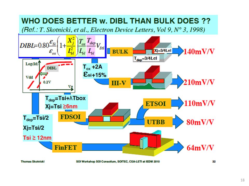
Electrostatics of FETs
BOX contributes to Tdep so make ultra thin UTBB allow the substrate (high doped) to be a second gate – Vt reduction Both in UTBB and FinFET xj and Tdep determined by geometry – not by doping channel can be left undoped Skotnicki, Future Fab, 2012
 to be a second gate – Vt reduction. Both in UTBB and FinFET. xj and Tdep determined by geometry – not by doping. channel can be left undoped. Skotnicki, Future Fab,")
6
Ultra-Thin-Body SOI MOSFET
The subthreshold leakage is reduced as the silicon film is made thinner. Tox=1.5nm, Nsub=1e15cm-3, Vdd=1V, Vgs=0 C. Hu

7
State-of-the-Art 5nm Thin-Body SOI
ETSOI, IBM K. Cheng et al, IEDM, 2009

8
Device Architecture Options => 3D
Planar SOI, FinFET SOI and FinFET bulk. Planar: Ultra thin body UTB (channel thickness) with raised S/D Low doped channel (no RDF) S/D optimization still needed FinFET on silicon bulk FinFET on SOI FinFET SOI Planar FDSOI FinFET bulk Many Challenges of each ot these designs Thickness uniformity on the SOI wafers must be controlled precisely Smart-Cut process gives ± 0.5 nm control
 with raised S/D. Low doped channel (no RDF) S/D optimization still needed. FinFET on silicon bulk. FinFET on SOI. FinFET SOI. Planar FDSOI. FinFET bulk. Many Challenges of each ot these designs. Thickness uniformity on the SOI wafers must be controlled precisely. Smart-Cut process gives ± 0.5 nm control.")
9
Producing Silicon-on-Insulator (SOI) Substrates
Initial Silicon wafer A and B Oxidize wafer A to grow SiO2 Implant hydrogen into wafer A Flip wafer A and place it on wafer B. Anneal at low temperature to fuse both wafers together. Use a second annealing step to form H2 bubbles and split wafer A. Polish the surface of the SOI wafer and use it as the substrate. Wafer A can be reused in the next SOI steps. The challenge is in the thin and uniform Si layer fabrication SOITEC

10
Device Architecture and Fabrication

11
Fabrication using SOI wafer
Hisamoto, 2000 Drain Current increases with # of fins

12
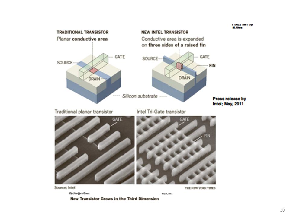
FinFETs are 3D Devices First FinFET in 1990 on SOI Wg<0.3 mm and Leff~0.57mm X-sections look like 2D devices – but it is “gate wrapped” around the fin!

13
3D and 2D cross-sectional potential contour plots at threshold (VGS = +0.2 V, VDS = 1.2 V) for SOI FinFET and bulk FinFET with Dxj = 10 nm. For both structures NB = 5 x1018 cm-3, Lg = Hfin = 50 nm, Wfin = 16 nm. 3D and 2D cross-sectional potential contour plots at threshold (VGS = 0.2 V, VDS = 1.2 V) for (a) SOI FinFET, (b) bulk FinFET with S/D junction depth misalignment of Dxj = 0 nm and (c) Dxj = 20 nm. With deeper junctions, potential barrier between the source and drain is lowered. Lg = Hfin = 50 nm, Wfin = 20 nm. Channel/body doping can be eliminated to mitigate RDF effects. • However, due to source/drain doping, a trade‐off exists between performance & RDF tolerance for Lg < 10nm M. Poljak et al. / Microelectronic Engineering 86 (2009) 2078–2085
 for (a) SOI FinFET, (b) bulk FinFET with S/D junction depth misalignment of Dxj = 0 nm and (c) Dxj = 20 nm. With deeper junctions, potential barrier between the source and drain is lowered. Lg = Hfin = 50 nm, Wfin = 20 nm. Channel/body doping can be eliminated to mitigate RDF effects. • However, due to source/drain doping, a trade‐off exists between. performance & RDF tolerance for Lg < 10nm. M. Poljak et al. / Microelectronic Engineering 86 (2009) 2078–2085.")
14
3D and 2D cross-sectional current density plots for SOI FinFET and bulk FinFET with Dxj = 10 nm. Both structures have NB = cm-3, Lg = Hfin = 50 nm, Wfin = 16 nm. VGS = +0.2 V, VDS = 1.2 V. The difference in on-state currents is caused by the corner effects.

15
Variations of FinFET Tall FinFET Short FinFET Nanowire FinFET Tall FinFET has the advantage of providing a large W and therefore large Ion while occupying a small footprint. Short FinFET has the advantage of less challenging lithography and etching. Nanowire FinFET gives the gate even more control over the silicon wire by surrounding it. C. Hu

16
The Gate‐all‐around (GAA) Structure Provides For The Greatest
Capacitive Coupling Between The Gate And The Channel. Singh et al., Si3N4 here Gates only on both sides Several multiple-gate FET concepts Mazurre &Celler, 2006

17
From Multi-gate MOSFET to Multi-fin FinFET
Eliminate deep leakage paths and provide gate control from more than one side of the channel. The Si film is very thin so that no leakage path is far from one of the gates. Because there are more than one gates, the structure may be called multi-gate MOSFET. Source Drain Gate 1 Vg Tox TSi Si Gate 2 double-gate SOI MOSFET

19
Issues and Challenges in Advanced FinFETs
Main cause of Vt Variation

20
Ed Nowak, IBM

21
Grow Si or high m fins Sivakumar, Intel

22
Sivakumar, Intel

23
Advantages and Disadvantages
Of SOI and Bulk FinFETs Sivakumar, Intel

25
Doping S/D regions difficult – 3D structure Shadowing effects
Isolation and wells for CMOS ?? Oxide Fill isolation Doping S/D regions difficult – 3D structure Shadowing effects Sivakumar, Intel

26
Challenges in Fins fabrication – Electric Field at the Corners – I-V distortion
Sivakumar, Intel

27
3D structure – shadowing in doping Use epitaxial growth – only on Si
SOI vs. Bulk FinFETs Source and Drains Doping of S/D regions: 3D structure – shadowing in doping Use epitaxial growth – only on Si Heteroepitaxy possible Sivakumar, Intel Iwai, 2011

28
FinFET Process Spacers fabrication Important challenging C. Hu

29
Spacers Formation to Leave Them at the Gate but not at the Fins

31
Iwai, 2011

32
Hybrid Orientation Technology - HOT
Mobility Booster Hybrid Orientation Technology - HOT Integrated process flow for the HOT CMOS fabrication on a hybridorientation substrate, where nFET is on the (100) surface and pFET is on the (110) surface. Yang et a;., IEEE 2006
 surface and pFET is on the (110) surface. Yang et a;., IEEE")
33
Mobility Boosters in SOI FETs
Schematic cross section of CMOS on hybrid-orientation substrates, including two types: type A with pFET on (110) SOI and nFET on (100) silicon epitaxial layer and type B with nFET on (100) SOI and pFET on (110) silicon epitaxial layer. Yang et a;., IEEE 2006
 SOI and nFET on (100) silicon epitaxial layer. and type B with nFET on (100) SOI and pFET on (110) silicon epitaxial layer. Yang et a;., IEEE")
34
Top Challenges for Multi-Gate Fin Transistors
Implement High Strain in Fins? Planar Ref= Highly strained 4-5x p-mobility enhancement High level of fin strain NOT published to date High Parasitics in Fin Transistors Narrow fins lead to high Rext Fin architecture may also lead to higher fringe capacitance Manufacturing worthy Patterning Fin, Gate and Spacer patterning will be extremely challenging in a manufacturing environment Design Device Z increments quantized J. Kavalieros et. al. VLSI Symp 2006 A. Dixit, K. Anil et al., Solid State Electronics, 2006 Best published drive currents for Multi-Gate Fin Transistors are significantly lower than best published planar transistors to date Many significant challenges remain to be resolved for Fin Transistors

Similar presentations


 Material of HW#12 & HW#13 (Lectures 33 through 38) –MOS non-idealities, V T adjustment;>")
 Transistors>")


![EE415 VLSI Design The Devices: MOS Transistor [Adapted from Rabaey’s Digital Integrated Circuits, ©2002, J. Rabaey et al.]](/16/5062541/big_thumb.jpg "EE415 VLSI Design The Devices: MOS Transistor [Adapted from Rabaey’s Digital Integrated Circuits, ©2002, J. Rabaey et al.]>")


