Download presentation
Presentation is loading. Please wait.

1
4 December 2002, ITRS 2002 Update Conference The International Technology Roadmap for Semiconductors 2002 Update Summary Overall Roadmap Technology Characteristics (ORTC) Overview 12/04/02 Alan Allan / Intel Corporation
 Overview 12/04/02 Alan Allan / Intel Corporation")
2
4 December 2002, ITRS 2002 Update Conference Key Messages The Technology Roadmap for Semiconductors has guided the R&D activities for the last 10 years! 2003 marks the year of 100nm or below: Welcome to the challenges of the Nanotechnology Era! NO CHANGES from the 2001 Scaling targets and Chip Size models– First Time Since 1994! –Economics (Chip Size) consistent with historical trends through 2004 –Performance (Frequency) consistent with historical trends through 2005 –Density (Functionality) consistent with historical trends through 2004 …..but need breakthroughs after 2005! We will continue to look for evidence of Industry Trend Acceleration/Deceleration in 2003
 consistent with historical trends through 2004 –Performance (Frequency) consistent with historical trends through 2005 –Density (Functionality) consistent with historical trends through 2004 …..but need breakthroughs after We will continue to look for evidence of Industry Trend Acceleration/Deceleration in")
3
4 December 2002, ITRS 2002 Update Conference Production Ramp-up Model and Technology Node Volume (Parts/Month) 1K 10K 100K Months 0 -24 1M 10M 100M Alpha Tool 1224 -12 DevelopmentProduction Beta Tool Production Tool First Conf. Papers First Two Companies Reaching Production Volume (Wafers/Month) 2 20 200 2K 20K 200K Source: 2001 ITRS - Exec. Summary 2002 ITRS Update – (No Changes from 2001 ITRS)
 K 20K 200K Source: 2001 ITRS - Exec. Summary 2002 ITRS Update – (No Changes from 2001 ITRS).")
4
4 December 2002, ITRS 2002 Update Conference MOS Transistor Scaling (1974 to present) S=0.7 [0.5x per 2 nodes] Pitch Gate
![4 December 2002, ITRS 2002 Update Conference MOS Transistor Scaling (1974 to present) S=0.7 [0.5x per 2 nodes] Pitch Gate](http://images.slideplayer.com/2/696546/slides/slide_4.jpg "4 December 2002, ITRS 2002 Update Conference MOS Transistor Scaling (1974 to present) S=0.7 [0.5x per 2 nodes] Pitch Gate")
5
4 December 2002, ITRS 2002 Update Conference 2002 ITRS Update – (No Changes from 2001 ITRS) SCALING Timing Highlights Technology Node and Industry Pace: The DRAM Half-Pitch (HP) on a 3-year-cycle trend after 130nm/2001 The MPU/ASIC HP remains on a 2-year-cycle trend until 90nm/2004, and then remains equal to DRAM HP (3-year cycle) The MPU Printed Gate Length (Pr GL ) and Physical Gate Length (Ph GL) will be on a 2-year-cycle until 45nm and 32nm, respectively, until the year 2005 The MPU Pr GL and Ph GL will proceed parallel to the DRAM/MPU HP trends on a 3-year cycle beyond the year 2005 The ASIC/Low Power Pr/Ph GL is delayed 2 years behind MPU Pr/Ph GL ASIC HP equal to MPU HP
 SCALING Timing Highlights Technology Node and Industry Pace: The DRAM Half-Pitch (HP) on a 3-year-cycle trend after 130nm/2001 The MPU/ASIC HP remains on a 2-year-cycle trend until 90nm/2004, and then remains equal to DRAM HP (3-year cycle) The MPU Printed Gate Length (Pr GL ) and Physical Gate Length (Ph GL) will be on a 2-year-cycle until 45nm and 32nm, respectively, until the year 2005 The MPU Pr GL and Ph GL will proceed parallel to the DRAM/MPU HP trends on a 3-year cycle beyond the year 2005 The ASIC/Low Power Pr/Ph GL is delayed 2 years behind MPU Pr/Ph GL ASIC HP equal to MPU HP")
6
4 December 2002, ITRS 2002 Update Conference Source: 2001 ITRS - Exec. Summary, ORTC 2002 ITRS Update – (No Changes from 2001 ITRS)
.")
7
4 December 2002, ITRS 2002 Update Conference Source: 2001 ITRS - Exec. Summary, ORTC 2002 ITRS Update – (No Changes from 2001 ITRS)
.")
8
1 10 100 1,000 10,000 100,000 19801985199019952000200520102015 Frequency (MHz) 2X / 4 Years 2X / 2 - 2½ Years 2X / 2½ Years MPU Clock Frequency Historical Trend: Gate Scaling, Transistor Design contributed ~ 17-19%/year Architectural Design innovation contributed additional ~ 21-13%/year Actual Scaling Acceleration, Or Equivalent Scaling Innovation Needed to maintain historical trend Historical 1999 ITRS 2001 ITRS MPU Clock Frequency Actual vs ITRS Sources: Sematech, 2001 ITRS ORTC 28 2002 ITRS Update – (No Changes from 2001 ITRS)
 2X / 4 Years 2X / 2 - 2½ Years 2X / 2½ Years MPU Clock Frequency Historical Trend: Gate Scaling, Transistor Design contributed ~ 17-19%/year Architectural Design innovation contributed additional ~ 21-13%/year Actual Scaling Acceleration, Or Equivalent Scaling Innovation Needed to maintain historical trend Historical 1999 ITRS 2001 ITRS MPU Clock Frequency Actual vs ITRS Sources: Sematech, 2001 ITRS ORTC ITRS Update – (No Changes from 2001 ITRS)")
9
4 December 2002, ITRS 2002 Update Conference 1.59/yr 1.41/yr 0.71/yr 0.74/yr 1.26/yr 1.47/yr 1.34/yr 2001 ITRS DRAM Model Trend Analysis (cont.) 2002 ITRS Update – (No Changes from 2001 ITRS)
 2002 ITRS Update – (No Changes from 2001 ITRS)")
10
4 December 2002, ITRS 2002 Update Conference 572mm2 Litho Field Size 286mm2 2 per Field Size 800mm2 Litho Field Size MPU Chip size (mm2) – Historical Trends vs 2001 ITRS Model* 1000 100 10 198019851990199520002005201020152020 CP MPU 140mm2 HP MPU 310mm2 CP Shrink 70mm2 * ITRS Design TWG MPU Transistors/Chip Model: ~2x/Node = 2x/2yrs from 1999 - 2001; then 2x/3yrs from 2001- 2016 *1999 Leading- Edge.18u CP MPU: 512KB (28Mt [58.3%] x 1.18u2/t = 34mm2) + 20Mt Logic x 5.19u2/t = 104mm2 + 2mm2 OH= 106mm2 = Total 48Mt x ave 2.92u2/t = 140mm2 *1999 Leading- Edge.18u HP MPU: 2MB (113Mt [81.9%] x 1.18u2/t = 135mm2) + 25Mt Logic x 5.19u2/t = 130mm2 + 45mm2 OH= 310mm2 = Total 138Mt x ave 2.25u2/t = 310mm2 2002 ITRS Update – (No Changes from 2001 ITRS)
![4 December 2002, ITRS 2002 Update Conference 572mm2 Litho Field Size 286mm2 2 per Field Size 800mm2 Litho Field Size MPU Chip size (mm2) – Historical Trends vs 2001 ITRS Model* CP MPU 140mm2 HP MPU 310mm2 CP Shrink 70mm2 * ITRS Design TWG MPU Transistors/Chip Model: ~2x/Node = 2x/2yrs from ; then 2x/3yrs from *1999 Leading- Edge.18u CP MPU: 512KB (28Mt [58.3%] x 1.18u2/t = 34mm2) + 20Mt Logic x 5.19u2/t = 104mm2 + 2mm2 OH= 106mm2 = Total 48Mt x ave 2.92u2/t = 140mm2 *1999 Leading- Edge.18u HP MPU: 2MB (113Mt [81.9%] x 1.18u2/t = 135mm2) + 25Mt Logic x 5.19u2/t = 130mm2 + 45mm2 OH= 310mm2 = Total 138Mt x ave 2.25u2/t = 310mm ITRS Update – (No Changes from 2001 ITRS)](http://images.slideplayer.com/2/696546/slides/slide_10.jpg "4 December 2002, ITRS 2002 Update Conference 572mm2 Litho Field Size 286mm2 2 per Field Size 800mm2 Litho Field Size MPU Chip size (mm2) – Historical Trends vs 2001 ITRS Model* CP MPU 140mm2 HP MPU 310mm2 CP Shrink 70mm2 * ITRS Design TWG MPU Transistors/Chip Model: ~2x/Node = 2x/2yrs from ; then 2x/3yrs from *1999 Leading- Edge.18u CP MPU: 512KB (28Mt [58.3%] x 1.18u2/t = 34mm2) + 20Mt Logic x 5.19u2/t = 104mm2 + 2mm2 OH= 106mm2 = Total 48Mt x ave 2.92u2/t = 140mm2 *1999 Leading- Edge.18u HP MPU: 2MB (113Mt [81.9%] x 1.18u2/t = 135mm2) + 25Mt Logic x 5.19u2/t = 130mm2 + 45mm2 OH= 310mm2 = Total 138Mt x ave 2.25u2/t = 310mm ITRS Update – (No Changes from 2001 ITRS)")
11
4 December 2002, ITRS 2002 Update Conference Density Trends (bits/cm2, t/cm2) – ITRS / ORTC 2002 ITRS Update – (No Changes from 2001 ITRS) ITRS 2001 Moores Law Targets: DRAM: 2x/2.5yrs; 1.05x/yr Chip Size MPU: 2x/node = 2x/3years; FLAT Chip Size
 – ITRS / ORTC 2002 ITRS Update – (No Changes from 2001 ITRS) ITRS 2001 Moores Law Targets: DRAM: 2x/2.5yrs; 1.05x/yr Chip Size MPU: 2x/node = 2x/3years; FLAT Chip Size")
12
4 December 2002, ITRS 2002 Update Conference Key Messages The Technology Roadmap for Semiconductors has guided the R&D activities for the last 10 years! 2003 marks the year of 100nm or below: Welcome to the challenges of the Nanotechnology Era! NO CHANGES from the 2001 Scaling targets and Chip Size models– First Time Since 1994! –Economics (Chip Size) consistent with historical trends through 2004 –Performance (Frequency) consistent with historical trends through 2005 –Density (Functionality) consistent with historical trends through 2004 …..but need breakthroughs after 2005! We will continue to look for evidence of Industry Trend Acceleration/Deceleration in 2003
 consistent with historical trends through 2004 –Performance (Frequency) consistent with historical trends through 2005 –Density (Functionality) consistent with historical trends through 2004 …..but need breakthroughs after We will continue to look for evidence of Industry Trend Acceleration/Deceleration in")
13
4 December 2002, ITRS 2002 Update Conference Backup

14
4 December 2002, ITRS 2002 Update Conference Production Definition

15
4 December 2002, ITRS 2002 Update Conference Technology Node vs Actual Wafer Production Capacity 0.01 0.1 1 10 1995 2000 2005 Year 19961997199820011999200420032002 W.P.C. Feature Size (Half Pitch) ( m) 0.01 0.1 1 10 1995 2000 2005 Year 19961997199820011999200420032002 W.P.C. ITRS Technology Node W.P.C.= Total Worldwide Wafer Production Capacity (Relative Value) Sources: 1995 to 1999: SICAS 2000: Yano Research Institute& SIRIJ Feature Size of Technology >0.7 m 0.4-0.7 m <0.4 m >0.8 m 0.5-0.8 m 0.35-0.5 m 0.25- 0.35 m 0.2 - 0.25 m 0.18 - 0.2 m <0.18 m For 1995-1999 For 2000 Source: 2001 ITRS - Exec. Summary 2002 ITRS Update – (No Changes from 2001 ITRS)
 ( m) Year W.P.C. ITRS Technology Node W.P.C.= Total Worldwide Wafer Production Capacity (Relative Value) Sources: 1995 to 1999: SICAS 2000: Yano Research Institute& SIRIJ Feature Size of Technology >0.7 m m <0.4 m >0.8 m m m m m m <0.18 m For For 2000 Source: 2001 ITRS - Exec. Summary 2002 ITRS Update – (No Changes from 2001 ITRS).")
16
4 December 2002, ITRS 2002 Update Conference Scaling – Technology Nodes

17
4 December 2002, ITRS 2002 Update Conference Half Pitch (= Pitch/2) Definition (Typical MPU/ASIC) (Typical DRAM) Poly Pitch Metal Pitch Source: 2001 ITRS - Exec. Summary 2002 ITRS Update – (No Changes from 2001 ITRS)
.")
18
4 December 2002, ITRS 2002 Update Conference Scaling Calculator + Node Cycle Time: 250 -> 180 -> 130 -> 90 -> 65 -> 45 -> 32 -> 22 -> 16 0.5x 0.7 x NN+1N+2 Node Cycle Time (T yrs): *CARR(T) = [(0.5)^(1/2T yrs)] - 1 CARR(3 yrs) = -10.9% CARR(2 yrs) = -15.9% * CARR(T) = Compound Annual Reduction Rate (@ cycle time period, T) Log Half-Pitch Linear Time 1994 NTRS -.7x/3yrs Actual -.7x/2yrs Source: 2001 ITRS - Exec. Summary 2002 ITRS Update – (No Changes from 2001 ITRS)
![4 December 2002, ITRS 2002 Update Conference Scaling Calculator + Node Cycle Time: 250 -> 180 -> 130 -> 90 -> 65 -> 45 -> 32 -> 22 -> x 0.7 x NN+1N+2 Node Cycle Time (T yrs): *CARR(T) = [(0.5)^(1/2T yrs)] - 1 CARR(3 yrs) = -10.9% CARR(2 yrs) = -15.9% * CARR(T) = Compound Annual Reduction Rate cycle time period, T) Log Half-Pitch Linear Time 1994 NTRS -.7x/3yrs Actual -.7x/2yrs Source: 2001 ITRS - Exec.](http://images.slideplayer.com/2/696546/slides/slide_18.jpg "Summary 2002 ITRS Update – (No Changes from 2001 ITRS).")
19
4 December 2002, ITRS 2002 Update Conference 2001 ITRS ORTC Node Tables – w/Node Cycles [3-Year Node Cycle] [2-year cycle][3-year cycle] [Node = DRAM Half-Pitch (HP)] [MPU Gate Length Cycle (GL)]: [MPU HP/GL Cycle]: 2002 ITRS Update – (No Changes from 2001 ITRS)
![4 December 2002, ITRS 2002 Update Conference 2001 ITRS ORTC Node Tables – w/Node Cycles [3-Year Node Cycle] [2-year cycle][3-year cycle] [Node = DRAM Half-Pitch (HP)] [MPU Gate Length Cycle (GL)]: [MPU HP/GL Cycle]: 2002 ITRS Update – (No Changes from 2001 ITRS)](http://images.slideplayer.com/2/696546/slides/slide_19.jpg "4 December 2002, ITRS 2002 Update Conference 2001 ITRS ORTC Node Tables – w/Node Cycles [3-Year Node Cycle] [2-year cycle][3-year cycle] [Node = DRAM Half-Pitch (HP)] [MPU Gate Length Cycle (GL)]: [MPU HP/GL Cycle]: 2002 ITRS Update – (No Changes from 2001 ITRS)")
20
4 December 2002, ITRS 2002 Update Conference 2001 ITRS ORTC MPU Frequency Tables – w/Node Cycles Table 4c Performance and Package Chips: Frequency On-Chip Wiring LevelsNear-Term Years Y EAR OF P RODUCTION 2001 2002 2003 2004 2005 2006 2007 DRAM ½ Pitch (nm) 130 115 100 90 80 70 65 MPU/ASIC ½ Pitch (nm) 150 130 107 90 80 70 65 MPU Printed Gate Length (nm) 90 75 65 53 45 40 35 MPU Physical Gate Length (nm) 65 53 45 37 32 28 25 Chip Frequency (MHz) On - chip local clock 1,684 2,317 3,088 3,990 5,173 5,631 6,739 Chip - to-board (off-chip) speed (high-performance, for peripheral buses)[1] 1,684 2,317 3,088 3,990 5,173 5,631 6,739 Maximum number wiring levelsmaximum 7 8 8 8 9 9 9 Maximum number wiring levelsminimum 7 7 8 8 8 9 9 Table 4d Performance and Package Chips: Frequency, On-Chip Wiring LevelsLong-term Years Y EAR OF P RODUCTION 2010 2013 2016 DRAM ½ Pitch (nm) 45 32 22 MPU/ASIC ½ Pitch (nm) 45 32 22 MPU Printed Gate Length (nm) 25 18 13 MPU Physical Gate Length (nm) 18 13 9 Chip Frequency (MHz) On - chip local clock 11,511 19,348 28,751 Chip-to-board (off-chip) speed (high-performance, for peripheral buses)[1] 11,511 19,348 28,751 Maximum number wiring levelsmaximum 10 Maximum number wiring levelsminimum 9 9 10 [2-Yr GL Cycle; then 3-Yr] [3-year cycle] Sources: 2001 ITRS ORTC [MPU Gate Length Cycle (GL)]: 2002 ITRS Update – (No Changes from 2001 ITRS)
![4 December 2002, ITRS 2002 Update Conference 2001 ITRS ORTC MPU Frequency Tables – w/Node Cycles Table 4c Performance and Package Chips: Frequency On-Chip Wiring LevelsNear-Term Years Y EAR OF P RODUCTION DRAM ½ Pitch (nm) MPU/ASIC ½ Pitch (nm) MPU Printed Gate Length (nm) MPU Physical Gate Length (nm) Chip Frequency (MHz) On - chip local clock 1,684 2,317 3,088 3,990 5,173 5,631 6,739 Chip - to-board (off-chip) speed (high-performance, for peripheral buses)[1] 1,684 2,317 3,088 3,990 5,173 5,631 6,739 Maximum number wiring levelsmaximum Maximum number wiring levelsminimum Table 4d Performance and Package Chips: Frequency, On-Chip Wiring LevelsLong-term Years Y EAR OF P RODUCTION DRAM ½ Pitch (nm) MPU/ASIC ½ Pitch (nm) MPU Printed Gate Length (nm) MPU Physical Gate Length (nm) Chip Frequency (MHz) On - chip local clock 11,511 19,348 28,751 Chip-to-board (off-chip) speed (high-performance, for peripheral buses)[1] 11,511 19,348 28,751 Maximum number wiring levelsmaximum 10 Maximum number wiring levelsminimum [2-Yr GL Cycle; then 3-Yr] [3-year cycle] Sources: 2001 ITRS ORTC [MPU Gate Length Cycle (GL)]: 2002 ITRS Update – (No Changes from 2001 ITRS)](http://images.slideplayer.com/2/696546/slides/slide_20.jpg "4 December 2002, ITRS 2002 Update Conference 2001 ITRS ORTC MPU Frequency Tables – w/Node Cycles Table 4c Performance and Package Chips: Frequency On-Chip Wiring LevelsNear-Term Years Y EAR OF P RODUCTION DRAM ½ Pitch (nm) MPU/ASIC ½ Pitch (nm) MPU Printed Gate Length (nm) MPU Physical Gate Length (nm) Chip Frequency (MHz) On - chip local clock 1,684 2,317 3,088 3,990 5,173 5,631 6,739 Chip - to-board (off-chip) speed (high-performance, for peripheral buses)[1] 1,684 2,317 3,088 3,990 5,173 5,631 6,739 Maximum number wiring levelsmaximum Maximum number wiring levelsminimum Table 4d Performance and Package Chips: Frequency, On-Chip Wiring LevelsLong-term Years Y EAR OF P RODUCTION DRAM ½ Pitch (nm) MPU/ASIC ½ Pitch (nm) MPU Printed Gate Length (nm) MPU Physical Gate Length (nm) Chip Frequency (MHz) On - chip local clock 11,511 19,348 28,751 Chip-to-board (off-chip) speed (high-performance, for peripheral buses)[1] 11,511 19,348 28,751 Maximum number wiring levelsmaximum 10 Maximum number wiring levelsminimum [2-Yr GL Cycle; then 3-Yr] [3-year cycle] Sources: 2001 ITRS ORTC [MPU Gate Length Cycle (GL)]: 2002 ITRS Update – (No Changes from 2001 ITRS)")
21
4 December 2002, ITRS 2002 Update Conference Chip Size Trends

22
4 December 2002, ITRS 2002 Update Conference Chip Size Model Calculation Illustration - DRAM (Cell Array Area / Chip Size) x 100 = Cell Array Efficiency (%): Chip Size = (A x f 2 x Nbits)/CAE f 2 Cell Area = Cell Area Factor (A) x f 2 ; f = technology node (half-pitch) feature size; Example: Cell Area = 2x4 x f 2 = 8 f 2 Cell Array Area = Cell Area x number of bits (2 n )
 x 100 = Cell Array Efficiency (%): Chip Size = (A x f 2 x Nbits)/CAE f 2 Cell Area = Cell Area Factor (A) x f 2 ; f = technology node (half-pitch) feature size; Example: Cell Area = 2x4 x f 2 = 8 f 2 Cell Array Area = Cell Area x number of bits (2 n )")
23
4 December 2002, ITRS 2002 Update Conference 2001 ITRS DRAM Model Trend Analysis 3-yr Node Cycle vs 2-yr 0.89/yr 0.95/yr 0.71/yr 0.74/yr 2002 ITRS Update – (No Changes from 2001 ITRS) [Cell Design Improvement Factor]
![4 December 2002, ITRS 2002 Update Conference 2001 ITRS DRAM Model Trend Analysis 3-yr Node Cycle vs 2-yr 0.89/yr 0.95/yr 0.71/yr 0.74/yr 2002 ITRS Update – (No Changes from 2001 ITRS) [Cell Design Improvement Factor]](http://images.slideplayer.com/2/696546/slides/slide_23.jpg "4 December 2002, ITRS 2002 Update Conference 2001 ITRS DRAM Model Trend Analysis 3-yr Node Cycle vs 2-yr 0.89/yr 0.95/yr 0.71/yr 0.74/yr 2002 ITRS Update – (No Changes from 2001 ITRS) [Cell Design Improvement Factor]")
24
4 December 2002, ITRS 2002 Update Conference DRAM Cell Area History / 2001 ITRS Model DRAM Cell Area 0.001 0.01 0.1 1 10 19861989199219951998200120042007201020132016 Year Cell Area (u2) History <--2000 --> F'cast 1Gb / 2Gb CAF (A) = 6 4Gb / 8Gb CAF (A) = 6 16Gb / 32Gb CAF (A) = 4 64 Gb/128Gb CAF (A) = 4 64 Mb CAF (A) = 11 = 1.3/.35^2;.71/.25^2 16->10 (per FEP) 4 Mb CAF (A) = 22 = 11/.71^2 26 (per FEP) 16 Mb CAF (A) = 16 = 4.0/.5^2 21 (per FEP) 1 Mb (est.) CAF (A) = 31 = 31/1.0^2 29 (per FEP) 128/256Mb CAF (A) = 8.0 =.35/.21^2;.26/.18^2 10 -> 8 (per FEP) Actual Scaling Acceleration, Or Equivalent Scaling Innovation Needed to maintain historical trend DRAM Cell Size Historical Trend: Half-Pitch Scaling, contributed ~.5x / 3 years [(.7x)^2] Cell Design innovation contributed additional ~.7x / 3 years 0.35x / 3 Years –29%/yr Historical Actual 2001 ITRS Sources: Sematech, 2001 ITRS ORTC 512Mb 2002 ITRS Update – (No Changes from 2001 ITRS)
![4 December 2002, ITRS 2002 Update Conference DRAM Cell Area History / 2001 ITRS Model DRAM Cell Area Year Cell Area (u2) History < > F cast 1Gb / 2Gb CAF (A) = 6 4Gb / 8Gb CAF (A) = 6 16Gb / 32Gb CAF (A) = 4 64 Gb/128Gb CAF (A) = 4 64 Mb CAF (A) = 11 = 1.3/.35^2;.71/.25^2 16->10 (per FEP) 4 Mb CAF (A) = 22 = 11/.71^2 26 (per FEP) 16 Mb CAF (A) = 16 = 4.0/.5^2 21 (per FEP) 1 Mb (est.) CAF (A) = 31 = 31/1.0^2 29 (per FEP) 128/256Mb CAF (A) = 8.0 =.35/.21^2;.26/.18^2 10 -> 8 (per FEP) Actual Scaling Acceleration, Or Equivalent Scaling Innovation Needed to maintain historical trend DRAM Cell Size Historical Trend: Half-Pitch Scaling, contributed ~.5x / 3 years [(.7x)^2] Cell Design innovation contributed additional ~.7x / 3 years 0.35x / 3 Years –29%/yr Historical Actual 2001 ITRS Sources: Sematech, 2001 ITRS ORTC 512Mb 2002 ITRS Update – (No Changes from 2001 ITRS)](http://images.slideplayer.com/2/696546/slides/slide_24.jpg "4 December 2002, ITRS 2002 Update Conference DRAM Cell Area History / 2001 ITRS Model DRAM Cell Area Year Cell Area (u2) History < > F cast 1Gb / 2Gb CAF (A) = 6 4Gb / 8Gb CAF (A) = 6 16Gb / 32Gb CAF (A) = 4 64 Gb/128Gb CAF (A) = 4 64 Mb CAF (A) = 11 = 1.3/.35^2;.71/.25^2 16->10 (per FEP) 4 Mb CAF (A) = 22 = 11/.71^2 26 (per FEP) 16 Mb CAF (A) = 16 = 4.0/.5^2 21 (per FEP) 1 Mb (est.) CAF (A) = 31 = 31/1.0^2 29 (per FEP) 128/256Mb CAF (A) = 8.0 =.35/.21^2;.26/.18^2 10 -> 8 (per FEP) Actual Scaling Acceleration, Or Equivalent Scaling Innovation Needed to maintain historical trend DRAM Cell Size Historical Trend: Half-Pitch Scaling, contributed ~.5x / 3 years [(.7x)^2] Cell Design innovation contributed additional ~.7x / 3 years 0.35x / 3 Years –29%/yr Historical Actual 2001 ITRS Sources: Sematech, 2001 ITRS ORTC 512Mb 2002 ITRS Update – (No Changes from 2001 ITRS)")
25
4 December 2002, ITRS 2002 Update Conference ORTC Table TWG Line Item Ownership Chk's by L. Wilson/A.Allan ORTC Table TWG Owner TWG Table - Table 1a-dDRAM Model FEP [DRAM Model] -no change - Table 1f-jMPU Model Design [MPU Model] -no change - Table 2a,bLitho Field Size Table unchgd Litho57a,b Table not changed Wafer Size line item unchgd FEP, FI50a,b AA to review-done-no change - Table 3a,b# of Chip I/Os Table unchgd Test, Design24a,b Table not changed # of Package Pins Table unchgd Test, A&P25a,b Table not changed # of Package Balls HP updtd-NOchg to# A&P, Test75a,b AA to confirm-done-no change - Table 4a,bChip Pad Pitch Flip chip area array updtd A&P77 AA to confirm -done/updated Cost-Per-Pin Low Cost updtd A&P75a,b AA to confirm -done/updated - Table4c,dChip Frequency Design, PIDs[MPU Model] -no change Chip-to-Board Frequency Design, A&P[MPU Model] -no change Max # Wire Levels line item unchgd Interconnect62a,b AA to review- done/corrections - Table 5a,bElectrical Defects Yield Enhance. - Table 6a,bP.Supply Volt. line item unchgd PIDs 35a,b AA to review-done-no change Max. Power CP & HP updtd -NOchg to# A&P, Design, PIDs 75a,b AA to confirm -done-no change - Table 7a,bAffordable Cost Economic (AA actg)n/a -no change Test Cost Table unchgd Test24a,b Table not changed 90, 91 only notes AA to review –done -no change ORTC Table Line Item(s)
n/a -no change Test Cost Table unchgd Test24a,b Table not changed 90, 91 only notes AA to review –done -no change ORTC Table Line Item(s).")
26
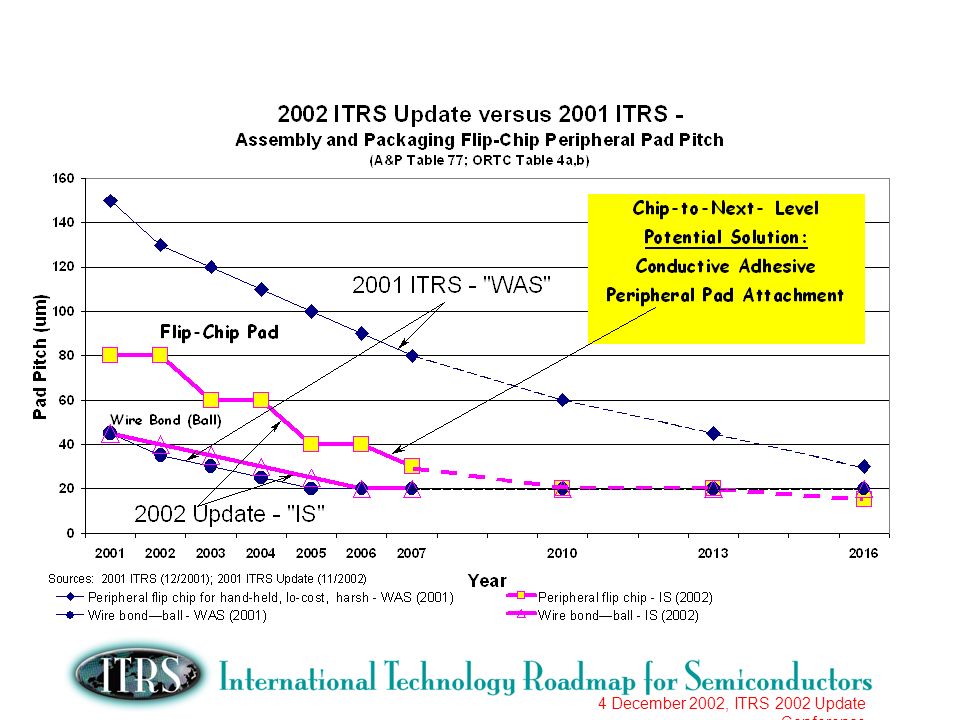
4 December 2002, ITRS 2002 Update Conference 2002 Update vs 2001 ITRS Example: ORTC Line Item Update: A&P Chip-to-Next-Level (ORTC Table 4a,b; A&P Table 77)
")
27
4 December 2002, ITRS 2002 Update Conference Assembly and Packaging – 2002 Update vs. 2001

28
4 December 2002, ITRS 2002 Update Conference

Similar presentations