Download presentation
Presentation is loading. Please wait.

1
GPGPU Ing. Martino Ruggiero Ing. Andrea Marongiu
2
Old and New Wisdom in Computer Architecture
Old: Power is free, Transistors are expensive New: “Power wall”, Power expensive, Transistors free (Can put more transistors on chip than can afford to turn on) Old: Multiplies are slow, Memory access is fast New: “Memory wall”, Multiplies fast, Memory slow (200 clocks to DRAM memory, 4 clocks for FP multiply) Old: Increasing Instruction Level Parallelism via compilers, innovation (Out-of-order, speculation, VLIW, …) New: “ILP wall”, diminishing returns on more ILP HW (Explicit thread and data parallelism must be exploited) New: Power Wall + Memory Wall + ILP Wall = Brick Wall
 Old: Multiplies are slow, Memory access is fast. New: Memory wall , Multiplies fast, Memory slow. (200 clocks to DRAM memory, 4 clocks for FP multiply) Old: Increasing Instruction Level Parallelism via compilers, innovation (Out-of-order, speculation, VLIW, …) New: ILP wall , diminishing returns on more ILP HW. (Explicit thread and data parallelism must be exploited) New: Power Wall + Memory Wall + ILP Wall = Brick Wall.")
3
Uniprocessor Performance (SPECint)
")
4
SW Performance:

5
Instruction-Stream Based Processing

6
Data-Stream-Based Processing

7
Instruction- and Data-Streams

8
Architectures: Data–Processor Locality
Field Programmable Gate Array (FPGA) Compute by configuring Boolean functions and local memory Processor Array / Multi-core Processor Assemble many (simple) processors and memories on one chip Processor-in-Memory (PIM) Insert processing elements directly into RAM chips Stream Processor Create data locality through a hierarchy of memories Graphics Processor Unit (GPU) Hide data access latencies by keeping 1000s of threads in-flight GPUs often excel in the performance/price ratio
 Compute by configuring Boolean functions and local memory. Processor Array / Multi-core Processor. Assemble many (simple) processors and memories on one chip. Processor-in-Memory (PIM) Insert processing elements directly into RAM chips. Stream Processor. Create data locality through a hierarchy of memories. Graphics Processor Unit (GPU) Hide data access latencies by keeping 1000s of threads in-flight. GPUs often excel in the performance/price ratio.")
9
Graphics Processing Unit (GPU)
Development driven by the multi-billion dollar game industry Bigger than Hollywood Need for physics, AI and complex lighting models Impressive Flops / dollar performance Hardware has to be affordable Evolution speed surpasses Moore’s law Performance doubling approximately 6 months

10
What is GPGPU? The graphics processing unit (GPU) on commodity video cards has evolved into an extremely flexible and powerful processor Programmability Precision Power GPGPU: an emerging field seeking to harness GPUs for general-purpose computation other than 3D graphics GPU accelerates critical path of application Data parallel algorithms leverage GPU attributes Large data arrays, streaming throughput Fine-grain SIMD parallelism Low-latency floating point (FP) computation Applications – see //GPGPU.org Game effects (FX) physics, image processing Physical modeling, computational engineering, matrix algebra, convolution, correlation, sorting
 computation. Applications – see //GPGPU.org. Game effects (FX) physics, image processing. Physical modeling, computational engineering, matrix algebra, convolution, correlation, sorting.")
11
Motivation 1: Computational Power GPUs are fast…
GPUs are getting faster, faster

12
Motivation 2: Flexible, Precise and Cheap:
Modern GPUs are deeply programmable Solidifying high-level language support Modern GPUs support high precision 32 bit floating point throughout the pipeline High enough for many (not all) applications
 applications.")
13
Parallel Computing on a GPU
NVIDIA GPU Computing Architecture Via a separate HW interface In laptops, desktops, workstations, servers 8-series GPUs deliver 50 to 200 GFLOPS on compiled parallel C applications GPU parallelism is doubling every year Programming model scales transparently Programmable in C with CUDA tools Multithreaded SPMD model uses application data parallelism and thread parallelism GeForce 8800 Tesla D870 Tesla S870

14
Towards GPGPU The previous 3D GPU The modern 3D GPU
A fixed function graphics pipeline The modern 3D GPU A Programmable parallel processor NVIDIA’s Tesla and Fermi architectures Unifies the vertex and pixel processors

26
The evolution of the pipeline
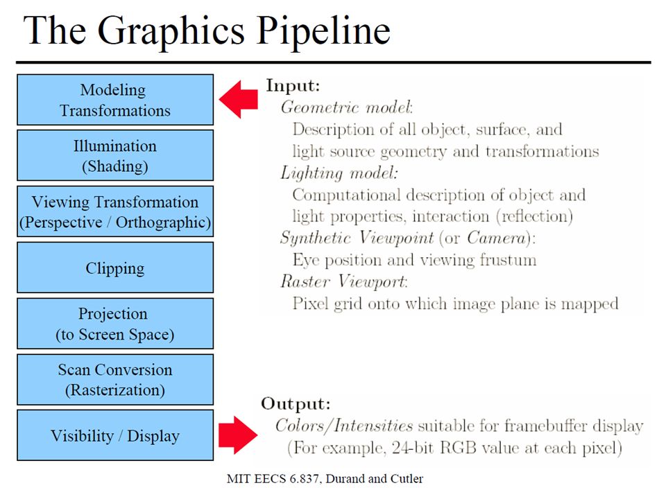
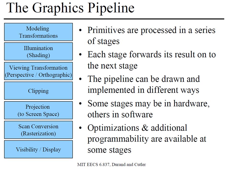
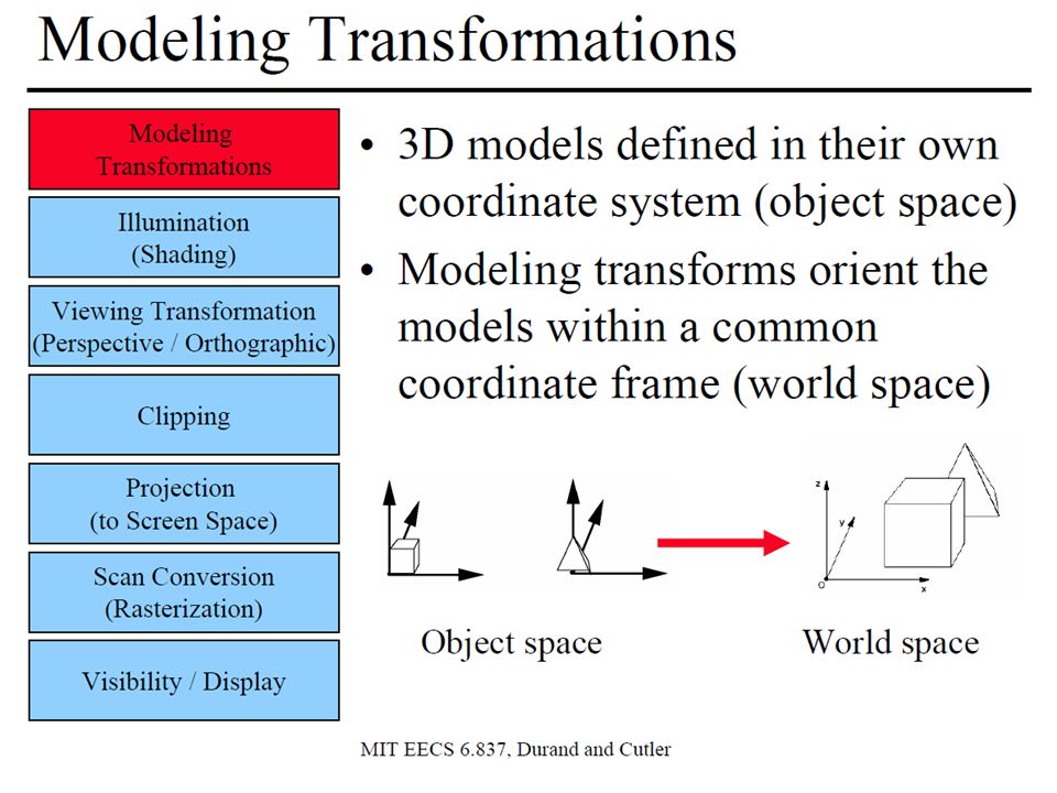
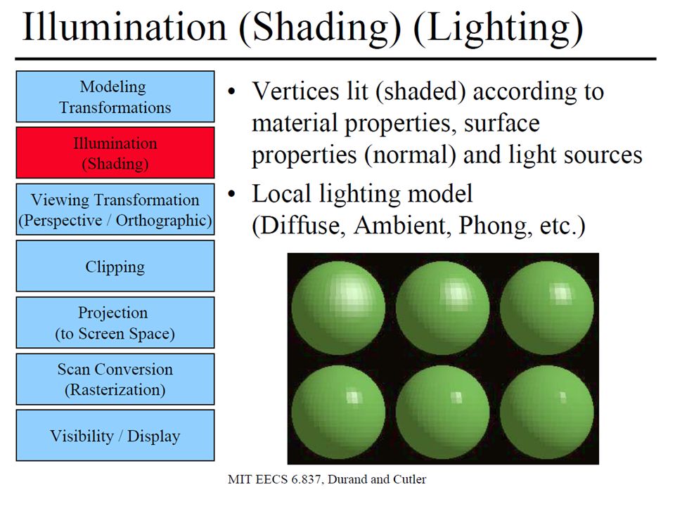
Elements of the graphics pipeline: A scene description: vertices, triangles, colors, lighting Transformations that map the scene to a camera viewpoint “Effects”: texturing, shadow mapping, lighting calculations Rasterizing: converting geometry into pixels Pixel processing: depth tests, stencil tests, and other per-pixel operations. Parameters controlling design of the pipeline: Where is the boundary between CPU and GPU ? What transfer method is used ? What resources are provided at each step ? What units can access which GPU memory elements ?

27
Generation I: 3dfx Voodoo (1996)
One of the first true 3D game cards Worked by supplementing standard 2D video card. Did not do vertex transformations: these were done in the CPU Did do texture mapping, z-buffering. Vertex Transforms Primitive Assembly Rasterization and Interpolation Raster Operations Frame Buffer CPU GPU PCI

28
Generation II: GeForce/Radeon 7500 (1998)
Main innovation: shifting the transformation and lighting calculations to the GPU Allowed multi-texturing: giving bump maps, light maps, and others.. Faster AGP bus instead of PCI Vertex Transforms Primitive Assembly Rasterization and Interpolation Raster Operations Frame Buffer GPU AGP

29
Generation III: GeForce3/Radeon 8500(2001)
For the first time, allowed limited amount of programmability in the vertex pipeline Also allowed volume texturing and multi-sampling (for antialiasing) Vertex Transforms Primitive Assembly Rasterization and Interpolation Raster Operations Frame Buffer GPU AGP Small vertex shaders
 Vertex. Transforms. Primitive. Assembly. Rasterization. and. Interpolation. Raster. Operations. Frame. Buffer. GPU. AGP. Small vertex. shaders.")
30
Generation IV: Radeon 9700/GeForce FX (2002)
This generation is the first generation of fully-programmable graphics cards Different versions have different resource limits on fragment/vertex programs Vertex Transforms Primitive Assembly Rasterization and Interpolation Raster Operations Frame Buffer AGP Programmable Vertex shader Programmable Fragment Processor

31
CPU-GPU Boundary (AGP/PCIe)
3D API Commands 3D API: OpenGL or Direct3D 3D Application Or Game CPU-GPU Boundary (AGP/PCIe) GPU Command & Data Stream Vertex Index Stream Pixel Location Stream Assembled Primitives Pixel Updates GPU Front End Primitive Assembly Rasterization and Interpolation Raster Operations Frame Buffer Pre-transformed Vertices Transformed Vertices Pre-transformed Fragments Transformed Fragments Programmable Vertex Processor Programmable Fragment Processor Vertex processors Operation on the vertices of primitives Points, lines, and triangles Typical Operations Transforming coordinates Setting up lighting and texture parameters Pixel processors Operation on rasterizer output Typical Operations Filling the interior of primitives
 GPU. Command & Data Stream. Vertex. Index. Stream. Pixel. Location. Stream. Assembled. Primitives. Pixel. Updates. GPU. Front End. Primitive. Assembly. Rasterization. and. Interpolation. Raster. Operations. Frame. Buffer. Pre-transformed. Vertices. Transformed. Vertices. Pre-transformed. Fragments. Transformed. Fragments. Programmable. Vertex. Processor. Programmable. Fragment. Processor. Vertex processors. Operation on the vertices of primitives. Points, lines, and triangles. Typical Operations. Transforming coordinates. Setting up lighting and texture parameters. Pixel processors. Operation on rasterizer output. Typical Operations. Filling the interior of primitives.")
32
The road to unification
Vertex and pixel processors have evolved at different rates Because GPUs typically must process more pixels than vertices, pixel-fragment processors traditionally outnumber vertex processors by about three to one. However, typical workloads are not well balanced, leading to inefficiency. For example, with large triangles, the vertex processors are mostly idle, while the pixel processors are fully busy. With small triangles, the opposite is true. The addition of more-complex primitive processing makes it much harder to select a fixed processor ratio. Increased generality Increased the design complexity, area and cost of developing two separate processors All these factors influenced the decision to design a unified architecture: to execute vertex and pixel-fragment shader programs on the same unified processor architecture.

33
Previous GPGPU Constraints

34
What’s wrong with GPGPU?

35
From pixel/fragment to thread program…
![]()
36
CPU style cores CPU-“style”

37
Slimming down

38
Two cores

39
Four cores

40
Sixteen cores

41
Add ALUs

42
128 elements in parallel

43
But what about branches?

44
But what about branches?

45
But what about branches?

46
But what about branches?

47
Clarification SIMD processing does not imply SIMD instructions
Option 1: Explicit vector instructions–Intel/AMD x86 SSE, Intel Larrabee Option 2: Scalar instructions, implicit HW vectorization HW determines instruction stream sharing across ALUs (amount of sharing hidden from software) NVIDIA GeForce (“SIMT”warps), ATI Radeon architectures
 NVIDIA GeForce ( SIMT warps), ATI Radeon architectures.")
48
Stalls! Stalls occur when a core cannot run the next instruction because of a dependency on a previous operation. Memory access latency = 100’s to 1000’s of cycles We’ve removed the fancy caches and logic that helps avoid stalls. But we have LOTS of independent work items. Idea #3: Interleave processing of many elements on a single core to avoid stalls caused by high latency operations.

49
Hiding stalls

50
Hiding stalls

51
Hiding stalls

52
Hiding stalls

53
Hiding stalls

54
Throughput!

55
Summary: Three key ideas
Use many “slimmed down cores”to run in parallel Pack cores full of ALUs(by sharing instruction stream across groups of work items) Avoid latency stalls by interleaving execution of many groups of workitems/ threads/ ... When one group stalls, work on another group
 Avoid latency stalls by interleaving execution of many groups of workitems/ threads/ ... When one group stalls, work on another group.")
56
Global memory

57
Parallel data cache

58
NVIDIA Tesla

59
CUDA Device Memory Space Overview
Each thread can: R/W per-thread registers R/W per-thread local memory R/W per-block shared memory R/W per-grid global memory Read only per-grid constant memory Read only per-grid texture memory (Device) Grid Constant Memory Texture Global Block (0, 0) Shared Memory Local Thread (0, 0) Registers Thread (1, 0) Block (1, 0) Host The host can R/W global, constant, and texture memories
 Grid. Constant. Memory. Texture. Global. Block (0, 0) Shared Memory. Local. Thread (0, 0) Registers. Thread (1, 0) Block (1, 0) Host. The host can R/W global, constant, and texture memories.")
60
Global, Constant, and Texture Memories (Long Latency Accesses)
Global memory Main means of communicating R/W Data between host and device Contents visible to all threads Texture and Constant Memories Constants initialized by host (Device) Grid Constant Memory Texture Global Block (0, 0) Shared Memory Local Thread (0, 0) Registers Thread (1, 0) Block (1, 0) Host
 Grid. Constant. Memory. Texture. Global. Block (0, 0) Shared Memory. Local. Thread (0, 0) Registers. Thread (1, 0) Block (1, 0) Host.")
61
Memory Hierarchy CPU and GPU Memory Hierarchy Disk CPU Main Memory
Slow CPU Caches GPU Video Memory CPU Registers GPU Caches GPU Constant Registers GPU Temporary Registers

62
NVIDIA’s Fermi Generation CUDA Compute Architecture:
The key architectural highlights of Fermi are: Third Generation Streaming Multiprocessor (SM) 32 CUDA cores per SM, 4x over GT200 8x the peak double precision floating point performance over GT200 Second Generation Parallel Thread Execution ISA Unified Address Space with Full C++ Support Optimized for OpenCL and DirectCompute Improved Memory Subsystem NVIDIA Parallel DataCache hierarchy with Configurable L1 and Unified L2 Caches improved atomic memory op performance NVIDIA GigaThreadTM Engine 10x faster application context switching Concurrent kernel execution Out of Order thread block execution Dual overlapped memory transfer engines
 32 CUDA cores per SM, 4x over GT200. 8x the peak double precision floating point performance over GT200. Second Generation Parallel Thread Execution ISA. Unified Address Space with Full C++ Support. Optimized for OpenCL and DirectCompute. Improved Memory Subsystem. NVIDIA Parallel DataCache hierarchy with Configurable L1 and Unified L2 Caches. improved atomic memory op performance. NVIDIA GigaThreadTM Engine. 10x faster application context switching. Concurrent kernel execution. Out of Order thread block execution. Dual overlapped memory transfer engines.")
63
Third Generation Streaming Multiprocessor
512 High Performance CUDA cores Each SM features 32 CUDA processors Each CUDA processor has a fully pipelined integer arithmetic logic unit (ALU) and floating point unit (FPU) 16 Load/Store Units Each SM has 16 load/store units, allowing source and destination addresses to be calculated for sixteen threads per clock. Supporting units load and store the data at each address to cache or DRAM. Four Special Function Units Special Function Units (SFUs) execute transcendental instructions such as sin, cosine, reciprocal, and square root.
 and floating point unit (FPU) 16 Load/Store Units. Each SM has 16 load/store units, allowing source and destination addresses to be calculated for sixteen threads per clock. Supporting units load and store the data at each address to cache or DRAM. Four Special Function Units. Special Function Units (SFUs) execute transcendental instructions such as sin, cosine, reciprocal, and square root.")
64
Dual Warp Scheduler The SM schedules threads in groups of 32 parallel threads called warps. Each SM features two warp schedulers and two instruction dispatch units, allowing two warps to be issued and executed concurrently. Fermi’s dual warp scheduler selects two warps, and issues one instruction from each warp to a group of sixteen cores, sixteen load/store units, or four SFUs. Because warps execute independently, Fermi’s scheduler does not need to check for dependencies from within the instruction stream. Using this elegant model of dual-issue, Fermi achieves near peak hardware performance.

65
Second Generation Parallel Thread Execution ISA
PTX is a low level virtual machine and ISA designed to support the operations of a parallel thread processor. At program install time, PTX instructions are translated to machine instructions by the GPU driver. The primary goals of PTX are: Provide a stable ISA that spans multiple GPU generations Achieve full GPU performance in compiled applications Provide a machine-independent ISA for C, C++, Fortran, and other compiler targets. Provide a code distribution ISA for application and middleware developers Provide a common ISA for optimizing code generators and translators, which map PTX to specific target machines. Facilitate hand-coding of libraries and performance kernels Provide a scalable programming model that spans GPU sizes from a few cores to many parallel cores

66
Fermi and the PTX 2.0 ISA address space
Three separate address spaces (thread private local, block shared, and global) for load and store operations. In PTX 1.0, load/store instructions were specific to one of the three address spaces; programs could load/ store values in a specific target address space known at compile time. difficult to fully implement C/C++ pointers since a pointer’s target address space may not be known at compile time. With PTX 2.0, a unified address space unifies all three address spaces into a single, continuous address space. 40-bit unified address space supports a Terabyte of addressable memory, and the load/store ISA supports 64-bit addressing for future growth.
 for load and store operations. In PTX 1.0, load/store instructions were specific to one of the three address spaces; programs could load/ store values in a specific target address space known at compile time. difficult to fully implement C/C++ pointers since a pointer’s target address space may not be known at compile time. With PTX 2.0, a unified address space unifies all three address spaces into a single, continuous address space. 40-bit unified address space supports a Terabyte of addressable memory, and the load/store ISA supports 64-bit addressing for future growth.")
67
Summary Table

Similar presentations