Download presentation
Presentation is loading. Please wait.

1
Solids and Bandstructure

2
QM of solids QM interference creates bandgaps and separates
metals from insulators and semiconductors

3
Recall numerical trick
y yn-1 yn yn+1 xn-1 xn xn+1 -t -t Un-1+2t -t t = ħ2/2ma2 H = -t Un+2t -t -t Un+1+2t -t Periodic BCs H(1,N)=H(N,1)=-t
=H(N,1)=-t.")
4
Extend now to infinite chain
1-D Solid e: Onsite energy (2t+U) -t: Coupling (off-diag. comp. of kinetic energy) -t e -t -t e -t H =
 -t: Coupling (off-diag. comp. of kinetic energy) -t e -t. -t e -t. H =")
5
Extend now to infinite chain
1-D Solid -t e -t -t e -t H = Let’s now find the eigenvalues of H for different matrix sizes N

6
Eigenspectra If we simply find eigenvalues of each NxN [H] and plot them in a sorted fashion, a band emerges! Note that it extends over a band-width of 4t (here t=1). The number of eigenvalues equals the size of [H] Note also that the energies bunch up near the edges, creating large DOS there N=
![Eigenspectra If we simply find eigenvalues of each NxN [H] and plot them in a sorted. fashion, a band emerges!](http://slideplayer.com/slide/6323774/21/images/6/Eigenspectra+If+we+simply+find+eigenvalues+of+each+NxN+%5BH%5D+and+plot+them+in+a+sorted.+fashion%2C+a+band+emerges%21.jpg "Note that it extends over a band-width of 4t (here t=1). The number of eigenvalues equals the size of [H] Note also that the energies bunch up near the edges, creating large DOS there. N=")
7
Eigenspectra How do we get a gap?
If we simply list the sorted eigenvalues vs their index, we get the plot below showing a continuous band of energies. How do we get a gap?

8
Dimerized Chain -t2 -t1 e H =
-t1 e -t2 -t2 e -t1 H = Once again, let’s do this numerically for various sized H

9
Eigenspectra If we keep the t’s different, two bands and a bandgap emerges Bandgap N= t1=1, t2=0.5

10
One way to create oscillations
+ Periodic nuclear potential (Kronig-Penney Model) Simpler abstraction
 Simpler abstraction.")
11
Solve numerically Un=Ewell/2[sign(sin(n/(N/(2*pi*periods))))+1];
Like Ptcle in a box but does not vanish at ends
![Solve numerically Un=Ewell/2[sign(sin(n/(N/(2*pi*periods))))+1];](http://slideplayer.com/slide/6323774/21/images/11/Solve+numerically+Un%3DEwell%2F2%5Bsign%28sin%28n%2F%28N%2F%282%2Api%2Aperiods%29%29%29%29%2B1%5D%3B.jpg "Like Ptcle in a box. but does not vanish. at ends.")
12
Matlab code hbar=1.054e-34;m=9.1e-31;q=1.6e-19;ang=1e-10; Ewell=10;
alpha0=sqrt(2*m*Ewell*q/hbar^2)*ang; period=2*pi/alpha0; periods=25;span=periods*period; N=505;a=span/(N+0.3); t0=hbar^2/(2*m*q*(a*ang)^2); n=linspace(1,N,N); Un=Ewell/2*(sign(sin(n/(N/(2*pi*periods))))+1); H=diag(Un)+2*t0*eye(N)-t0*diag(ones(1,N-1),1)-t0*diag(ones(1,N-1),-1); H(1,N)=-t0;H(N,1)=-t0; [v,d]=eig(H); [d,ind]=sort(real(diag(d)));v=v(:,ind); % figure(1) % plot(d/Ewell,'d','linewidth',3) % grid on % axis([ ]) figure(2) plot(n,Un); %axis([ ]) hold on for k=1:N plot(n,real(v(:,k))+d(k)/Ewell,'k','linewidth',3); axis([ ]) end
*ang; period=2*pi/alpha0; periods=25;span=periods*period; N=505;a=span/(N+0.3); t0=hbar^2/(2*m*q*(a*ang)^2); n=linspace(1,N,N); Un=Ewell/2*(sign(sin(n/(N/(2*pi*periods))))+1); H=diag(Un)+2*t0*eye(N)-t0*diag(ones(1,N-1),1)-t0*diag(ones(1,N-1),-1); H(1,N)=-t0;H(N,1)=-t0; [v,d]=eig(H); [d,ind]=sort(real(diag(d)));v=v(:,ind); % figure(1) % plot(d/Ewell, d , linewidth ,3) % grid on. % axis([ ]) figure(2) plot(n,Un); %axis([ ]) hold on. for k=1:N. plot(n,real(v(:,k))+d(k)/Ewell, k , linewidth ,3); axis([ ]) end.")
13
Bloch’s theorem y(x) = eikxu(x) y(x+a+b) = eik(a+b)y(x)
u(x+a+b) = u(x) y(x+a+b) = eik(a+b)y(x) Plane wave part eikx handles overall X-al Periodicity ‘Atomic’ part u(x) handles local bumps and wiggles
 = u(x) y(x+a+b) = eik(a+b)y(x) Plane wave part eikx. handles overall X-al. Periodicity. ‘Atomic’ part u(x) handles local bumps. and wiggles.")
14
Energy bands emerge E/Ewell ~ ~1-1.35 ~0.35

15
Can do this analytically, if we can survive the algebra
N domains 2N unknowns (A, B, C, Ds) Usual procedure Match y, dy/dx at each of the N-1 interfaces y(x ∞) = 0
 Usual procedure. Match y, dy/dx at each of the N-1 interfaces. y(x ∞) = 0.")
16
Can’t we exploit periodicity?
Bloch’s Theorem This means we can work over 1 period alone! Need periodic BCs at edges Solve transcendental equations graphically

17
Allowed energies appear in bands !
Like earlier, but folded into -p/(a+b) < k < p/(a+b) The graphical equation: Solutions subtended between black curve and red lines
 < k < p/(a+b) The graphical equation: Solutions subtended between. black curve and red lines.")
18
Number of states and Brillouin Zone
Only need points within BZ (outside, states repeat themselves on the atomic grid)
")
19
The overall solution looks like

20
More accurately...

21
Why do we get a gap? Let us start with a free electron in a periodic crystal, but ignore the atomic potentials for now At the interface (BZ), we have two counter-propagating waves eikx, with k = p/a, that Bragg reflect and form standing waves y E p/a -p/a Its periodically extended partner k
, we have two counter-propagating waves eikx, with k = p/a, that Bragg reflect and form standing waves. y E. p/a. -p/a. Its periodically. extended partner. k.")
22
Why do we get a gap? y+ y- y+ ~ cos(px/a) peaks at atomic sites
y- ~ sin(px/a) peaks in between E p/a -p/a Its periodically extended partner k
 peaks in between. E. p/a. -p/a. Its periodically. extended partner. k.")
23
Let’s now turn on the atomic potential
The y+ solution sees the atomic potential and increases its energy The y- solution does not see this potential (as it lies between atoms) Thus their energies separate and a gap appears at the BZ This happens only at the BZ where we have standing waves p/a -p/a y+ y- |U0| k
 Thus their energies separate and a gap appears at the BZ. This happens only at the BZ where we have standing waves. p/a. -p/a. y+ y- |U0| k.")
24
Nearly Free Electrons

25
What is the real-space velocity?
Superposition of nearby Bloch waves y(x) ≈ Aei(kx-Et/ħ) + Aei[(k+Dk)x-(E+DE)t/ħ] ≈ Aei(kx-Et/ħ)[1 + ei(Dkx-DEt/ħ)] Fast varying components Slowly varying envelope (‘beats’) k k+Dk time
 ≈ Aei(kx-Et/ħ) + Aei[(k+Dk)x-(E+DE)t/ħ] ≈ Aei(kx-Et/ħ)[1 + ei(Dkx-DEt/ħ)] Fast varying. components. Slowly varying. envelope (‘beats’) k. k+Dk. time.")
26
Band velocity Aei(kx-Et/ħ)[1 + ei(Dkx-DEt/ħ)] y(x) ≈
Envelope (wavepacket) moves at speed v = DE/ħDk = 1/ħ(∂E/∂k) i.e., Slope of E-k gives real-space velocity
![Band velocity Aei(kx-Et/ħ)[1 + ei(Dkx-DEt/ħ)] y(x) ≈](http://slideplayer.com/slide/6323774/21/images/26/Band+velocity+Aei%28kx-Et%2F%C4%A7%29%5B1+%2B+ei%28Dkx-DEt%2F%C4%A7%29%5D+y%28x%29+%E2%89%88.jpg "Envelope (wavepacket) moves at speed v = DE/ħDk = 1/ħ(∂E/∂k) i.e., Slope of E-k gives real-space velocity.")
27
Band velocity v = 1/ħ(∂E/∂k) Slope of E-k gives real-space velocity
This explains band-gap too! Two counterpropagating waves give zero net group velocity at BZ Since zero velocity means flat-band, the free electron parabola must distort at BZ Flat bands

28
Effective mass v = 1/ħ(∂E/∂k), p = ħk F = dp/dt = d(ħk)/dt
a = dv/dt = (dv/dk).(dk/dt) = 1/ħ2(∂2E/∂k2).F 1/m* = 1/ħ2(∂2E/∂k2) Curvature of E-k gives m*
.(dk/dt) = 1/ħ2(∂2E/∂k2).F. 1/m* = 1/ħ2(∂2E/∂k2) Curvature of E-k gives m*")
29
Approximations to bandstructure
Properties important near band tops/bottoms

30
What does Effective mass mean?
1/m* = 1/ħ2(∂2E/∂k2) Recall this is not a free particle but one moving in a periodic potential. But it looks like a free particle near the band-edges, albeit with an effective mass that parametrizes the difficulty faced by the electron in running thro’ the potential m* can be positive, negative, 0 or infinity!
 Recall this is not a free particle but. one moving in a periodic potential. But it looks like a free particle near the. band-edges, albeit with an effective mass. that parametrizes the difficulty faced by. the electron in running thro’ the potential. m* can be positive, negative, 0 or infinity!")
31
Band properties http://fermi.la.asu.edu/ccli/applets/kp/kp.html
Electronic wavefunctions overlap and their energies form bands

32
Els between bound and free

33
Band properties Electronic wavefunctions overlap
and their energies form bands

34
Band properties Shallower potentials give bigger overlaps.
Greater overlap creates greater bonding-antibonding splitting of each multiply degenerate level, creating wider bandwidths Since shallower potentials allow electrons to escape easier, they correspond to smaller effective mass Thus, effective mass ~ 1/bandwidth ~ 1/t (t: overlap)
")
35
Two opposite limits invoked to describe bands
Nearly free-electron model, Au, Ag, Al,... Parabolic electron bands distort near BZ to open bandgaps (slide 32) Tight-binding electrons, Fe, Co, Pd, Pt, ... Localized atomic states spill over so that their discrete energies expand into bands (slides 9, 38)
 Tight-binding electrons, Fe, Co, Pd, Pt, ... Localized atomic states spill over so that their. discrete energies expand into bands. (slides 9, 38)")
36
Electron and Hole fluxes
(For every positive J2 or J3 component, there is an equal negative one!)
")
37
Electron and Hole fluxes

38
How does m* look?

39
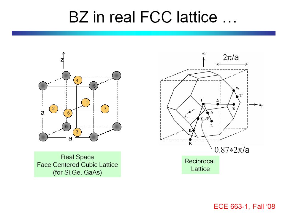
Xal structure in 1D (K: Fourier transform of real-space)
")
41
Bandstructure along G-X direction

42
Bandstructure along G-L direction

43
3D Bandstructures

44
GaAs Bandstructure

45
Constant Energy Surfaces for conduction band
Tensor effective mass

46
4-Valleys inside BZ of Ge

47
Valence band surfaces These are warped (derived from ‘p’ orbitals)
")
48
In summary Solution of Schrodinger equation tractable for
electrons in 1-D periodic potentials Electrons can only sit in specific energy bands. Effective mass and bandgap parametrize these states. Only a few bands (conduction and valence) contribute to conduction. Higher-d bands harder to visualize. Const energy ellipsoids help visualize where electrons sit
 contribute to conduction. Higher-d bands harder to visualize. Const energy ellipsoids help visualize where electrons sit.")
Similar presentations


 E(k) determines the dynamics of the electrons It is E(k) at the Fermi.>")


 Computers –Human based –Tube based –Solid state based Why do we need computers? –Modeling Analytical- great.>")

 First approximation.>")


